During AMD’s ‘together we advance_PCs’ event at the end of August, the company unveiled its Ryzen 7000 series of desktop processors, with four SKUs aimed at the mid-range and high-end market segments. After whetting the audience's appetites with that announcement, tomorrow AMD will be officially releasing their long-awaited next-generation CPUs.
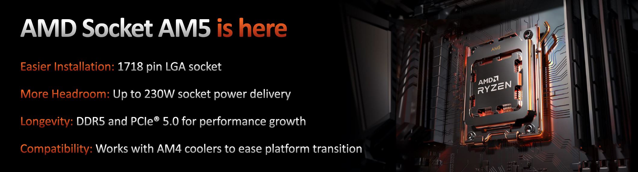
The launch of the Ryzen 7000 series brings a lot to digest, for casual fans and hardcore hardware enthusiasts alike. For their newest lineup of chips, AMD has given their desktop CPU platform a top-to-bottom update, not only releasing new CPUs, but releasing an entirely new platform, socket AM5 around it. As a result, for the first time in a few generations these chips are not drop-in compatible with existing AMD motherboards. But at the same time it has allowed AMD to deliver on a collection of platform improvements, ranging from DDR5 and PCIe 5.0 support to improved power management capabilities. AMD has even managed to sneak an entry-level Radeon RDNA2 architecture-based iGPU into the chip.
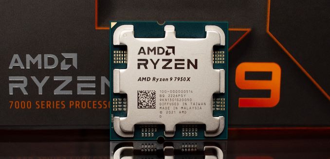
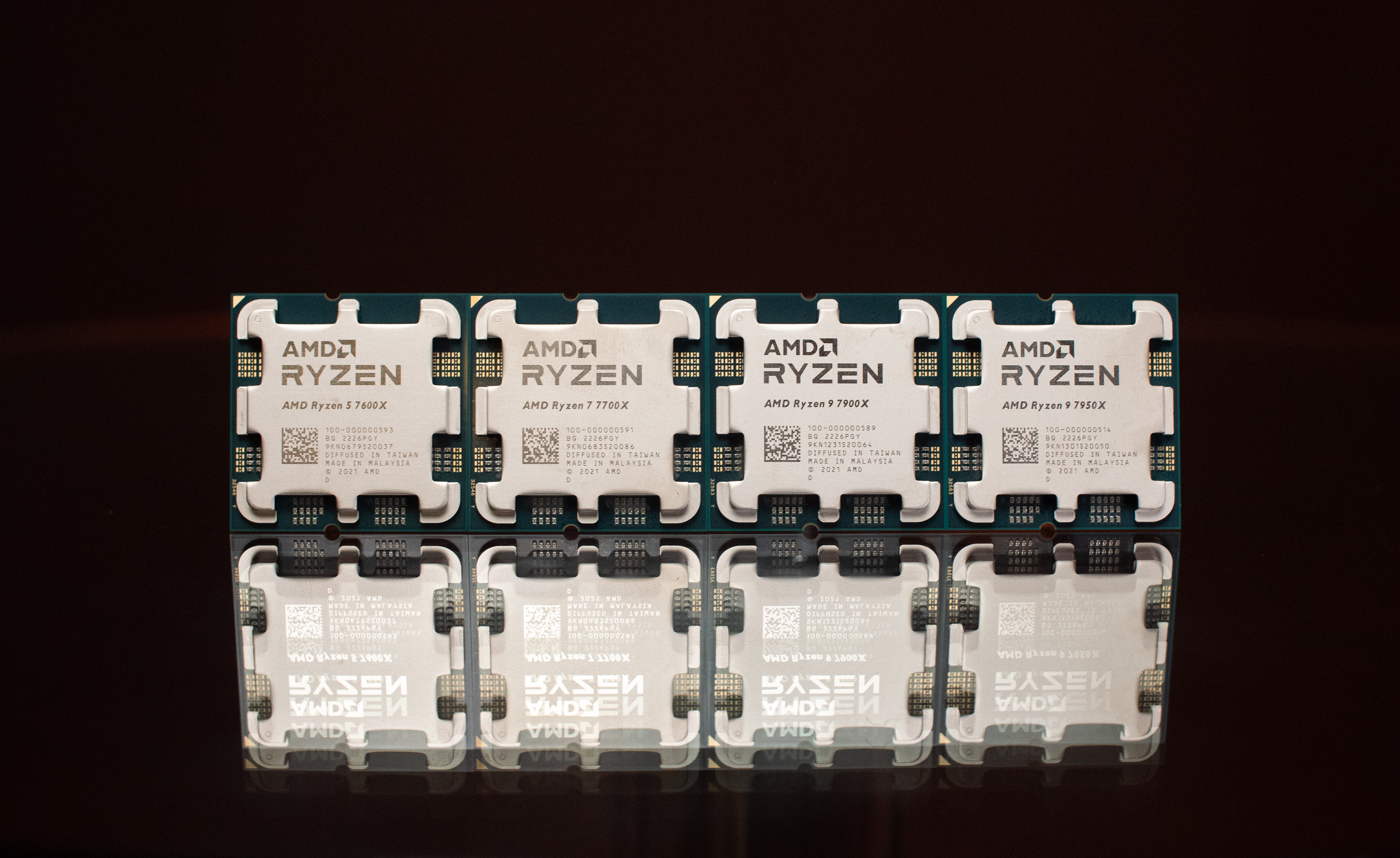
The Ryzen 9 7950X: 16 Cores, 32 Threads, New 170 W TDP: $699
We'll start, as always, with the CPUs themselves. AMD's flagship for this generation is the Ryzen 9 7950X, a 16 Zen 4 core CPU that AMD is looking to top the charts with for both single-threaded and multi-threaded workloads. The Ryzen 9 7950X has a base frequency of 4.5 GHz and a peak turbo clockspeed of 5.7 GHz, which makes it the highest clocked desktop x86 CPU to hit the market yet.
But don't think AMD's Zen 4 architecture is just about clockspeeds. AMD has also improved the IPC of their CPU architecture by an average of 13% – primarily relying on the addition of AVX-512 instruction support and comfortably larger caches and buffers throughout the CPU – which means that the Ryzen 7000 chips can deliver some significant performance improvements in a variety of single-threaded workloads.
As for multi-threaded workloads, AMD has been able to improve performance there as well, albeit with a reliance on both architecture improvements and higher TDPs to allow for higher sustained clockspeeds. One of the enabling factors here is that the AM5 platform allows for higher chip TDPs – up to 170W in the case of the 7950X – which is some 65W higher than the max TDPs on AMD's fastest 16 core Ryzen 5000 parts. As a result AMD is in a good position to deliver on the "leadership" class performance that the company is after, but not entirely for free.
The Ryzen 9 7900X, Ryzen 7 7700X, and Ryzen 5 7600X
Moving one down the stack is the Ryzen 9 7900X, which is a 12C/24T and 170W TDP part; it has a higher base frequency than the 7950X of 4.7 GHz, but with a slightly lower boost frequency of up to 5.6 GHz.
Below that, AMD has launched one Ryzen 7 part designed for mid-range desktop computing, the Ryzen 7 7700X. This is an 8C/16T SKU, with a boost frequency on a single core of up to 5.4 GHz, and a base frequency of 4.5 GHz. Notably, unlike the Ryzen 9 parts, this part has a more typical-for-AMD TDP of 105W.
Finally, also aimed at the mid-range market and the cheapest member of AMD's new product stack, we have the Ryzen 5 7600X. Offering 6C/12T with a TDP of 105W, the 7600X is Zen 4 at a more reasonable price point. The chip runs at a base frequency of 4.7 GHz, with a modest (compared to Ryzen 9) boost frequency on a single core of 5.3 GHz.
| AMD Ryzen 7000 versus Ryzen 5000 | |||||||
| AnandTech | Cores Threads |
Base Freq |
Turbo Freq |
Memory Support |
L3 Cache |
TDP | MSRP |
| Ryzen 9 7950X | 16C / 32T | 4.5GHz | 5.7GHz | DDR5-5200 | 64 MB | 170 W | $699 |
| Ryzen 9 5950X | 16C / 32T | 3.4 GHz | 4.9 GHz | DDR4-3200 | 64 MB | 105 W | $799 |
| Ryzen 9 7900X | 12C / 24T | 4.7GHz | 5.6GHz | DDR5-5200 | 64 MB | 170 W | $549 |
| Ryzen 9 5900X | 12C / 24T | 3.7 GHz | 4.8 GHz | DDR4-3200 | 64 MB | 105 W | $549 |
| Ryzen 7 7700X | 8C / 16T | 4.5GHz | 5.4GHz | DDR5-5200 | 32 MB | 105 W | $399 |
| Ryzen 7 5800X | 8C / 16T | 3.8 GHz | 4.7 GHz | DDR4-3200 | 32 MB | 105 W | $449 |
| Ryzen 5 7600X | 6C / 12T | 4.7GHz | 5.3GHz | DDR5-5200 | 32 MB | 105 W | $299 |
| Ryzen 5 5600X | 6C / 12T | 3.7 GHz | 4.6 GHz | DDR4-3200 | 32 MB | 65 W | $299 |
Comparing apples to apples, so to speak, between the new Ryzen 7000 series parts to the previous-generation Ryzen 5000 series parts, Ryzen 7000 has made some big overall improvements to the chips' capabilities. All of the Ryzen 7000 chips offer significant increases in both base and boost frequencies, which bodes well for overall performance. The worst we can say is that AMD hasn't increased their core counts at any price point/market segment, so all of the performance gains we'll see here today are entirely from architecture and clockspeeds, rather than the more immediate MT gains of throwing more silicon at the matter.
AMD's performance gains have been made possible in part through the Zen 4 architecture's superior power efficiency. While the Zen 4 architecture is modest refinement of Zen 3, delivering a 13% IPC improvement, it also gets the big advantage of being produced on TSMC's 5 nm process node, a full node's shrink from the TSMC 7nm process that was used for Ryzen 5000/3000. This efficiency has allowed AMD to boost clockspeeds without breaking the power bank, with the 105W TDP 7700X seeing a 700MHz improvement for no change in TDP. And multi-threaded performance is not left out in the cold, either; by increasing their top TDP to 170W, AMD is able to keep the CPU cores on their 12C and 16C parts at higher sustained turbo clocks, delivering much better performance there as well.
Of course one of the key arguments here is that more power calls for more cooling, which is very much true for the Ryzen 7000 series. Ryzen 7000’s TjMax for its Precision Boost Overdrive technology stands at 95°C, which means that the CPU will use all of the available thermal headroom right up to that point in order to maximize performance.
Although this can be overridden when manually overclocking, none the less the top-end Ryzen 7000 chips call for better cooling than their Ryzen 5000 counterparts. Users will need to employ more premium and aggressive coolers to squeeze every last drop of performance from Zen 4, as most of us are wont to do. AMD for their part has accounted for all of this with their design choices and product marketing, clearly advising Ryzen 9 79x0 owners to use a liquid cooler with these chips. Still, this does mean that AMD is not bundling their own CPU coolers with their retail SKUs, instead directing buyers to fairly powerful third-party coolers.
New AM5 Socket: AM4 Coolers will Support AM5 Too
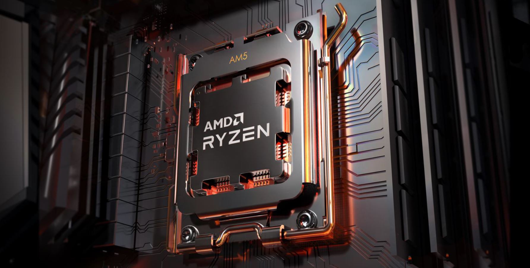
AMD has also transitioned to a new platform for Ryzen 7000, named AM5. Along with AM5 also comes a new socket, the titular socket AM5, a LGA-1718 socket that is AMD's first use of the LGA form factor for mainstream desktop CPUs. Now what’s interesting is AMD has specified that most AM4 coolers will support the new AM5 socket, which is great for keeping compatibility with existing coolers.
This also means that AM4 is slowly on its way to becoming a thing of the past. While AMD is still (many) months away from replacing their complete Ryzen 4000/5000 stack with Ryzen 7000 parts, today is the first day and the first step to doing so. None the less, AM4 does offer some incredible deals right now (e.g. 5800X3D), as well as support for cheaper DDR4 memory. This sits in contrast to the AM5 platform, which is entirely DDR5-only. Though when it comes to memory AMD does have a small advantage over Intel; whereas Intel's 12th Gen Core chips only support a maximum (JEDEC) speed of DDR5-4800, the Ryzen 7000 chips are officially rated for DDR5-5200.
To go with the new AM5 platform and provide motherboards for their new CPUs, AMD has unveiled four(ish) new chipsets. These are the B650 and X670, as well as their "Extreme" variations, the B650E and X670E. The top-end X670E series will feature both PCIe 5.0 lanes to the top PEG slot and support for PCIe 5.0 NVMe storage devices. The regular X670 chipset, on the other hand, foregoes the mandatory PCIe 5.0 speeds for the PEG slot in favor of easier-to-implement PCIe 4.0. In either case, both versions of X670 are intended to offer a plethora of I/O options, and in keeping with the general tiered structure of AMD's AM5 chipsets, X670 boards will generally offer better designs, better controllers, and better specifications.
The B650 chipsets, meanwhile, are designed to be more affordable, doing away with some of the I/O lanes and overall I/O flexibility the X670 chipsets enjoy. Like the Extreme X670, the B650E is intended for boards that will offer PCIe 5.0 to the PEG slot and NVMe storage. Otherwise, the lowest-tier B650 chipset dials that back to PCIe 4.0 for the PEG slot as well.
For this week's launch, only the X670/X670E boards will be available. Buyers looking for the cheaper B650/B650E boards will need to hold out until October.
New I/O Die: TSMC 6nm For Ryzen 7000
Last, as has been the case for the last couple of Ryzen desktop generations, for the Ryzen 7000 series AMD is constructing their CPUs out of chiplets. All Ryzen 7000 desktop chips are built from an I/O Die (IOD) as well as either one or two core complex dies (CCDs) depending on the SKU. The IOD hosts all of the PCIe 5.0 lanes, the DDR5 integrated memory controller (IMC), and new for Ryzen 7000, an integrated GPU based on AMD's Radeon RDNA2 GPU architecture. All things considered, the IOD used for the Ryzen 7000 is a pretty significant overhaul compared to AMD's previous IOD, with AMD implementing several new performance and power-saving features, as well as further cutting down on power consumption thanks to TSMC's 6nm process.
It’s time to dive deep into all of AMD’s new improvements and changes for its Zen 4 microarchitecture. Over the following pages we’ll, be going over the following:
- Ryzen 7000 Overview: Comparing Ryzen 7000 to Ryzen 5000 specifications
- Socket AM5: The New Platform For Consumer AMD
- More I/O For AM5: PCIe 5, Additional PCIe Lanes, & More Displays
- AM5 Chipsets: X670 and B650, Built by ASMedia
- DDR5 & AMD EXPO Memory: Memory Overclocking, AMD’s Way
- Ryzen 7000 I/O Die: TSMC & Integrated Graphics at Last
- Zen 4 Architecture: Power Efficiency, Performance, & New Instructions
- Zen 4 Execution Pipeline: Familiar Pipes With More Caching
- Test Bed and Setup
- Core-to-Core Latency
- SPEC2017 Single-Threaded Results
- SPEC2017 Multi-Threaded Results
- CPU Benchmark Performance: Power, Web, & Science
- CPU Benchmark Performance: Simulation and Encoding
- CPU Benchmark Performance: Rendering
- CPU Benchmark Performance: Legacy Tests
- Gaming Performance: 720p and Lower
- Gaming Performance: 1080p
- Gaming Performance: 4K
- Conclusion
While the star for most CPU launches is typically the titular CPU, there’s a good argument to be had that for the Ryzen 7000 desktop launch, AMD’s overall platform warrants just as much attention, if not a bit more. After all, the company’s up-to-now current AM4 platform was introduced back in 2016, alongside Bristol Ridge, the last of the Bulldozers. A lot has changed for AMD in the last 6 years – not the least being the movement to the Zen core family – and now their underlying platform is getting a major overhaul as well.
The first new consumer platform and associated socket designed by AMD since the start of the Zen era, AM5 is designed to bring three major updates to AMD’s desktop ecosystem. These can be roughly broken down as improving power delivery, adding DDR5 memory support, and boosting the amount of bandwidth and flexibility for I/O devices downstream of the CPU. All three of these things require (or at least are best accomplished) with CPU pin changes, so this is AMD’s first chance in 6 years to overhaul everything that flows in and out of their desktop CPUs.
Socket AM5
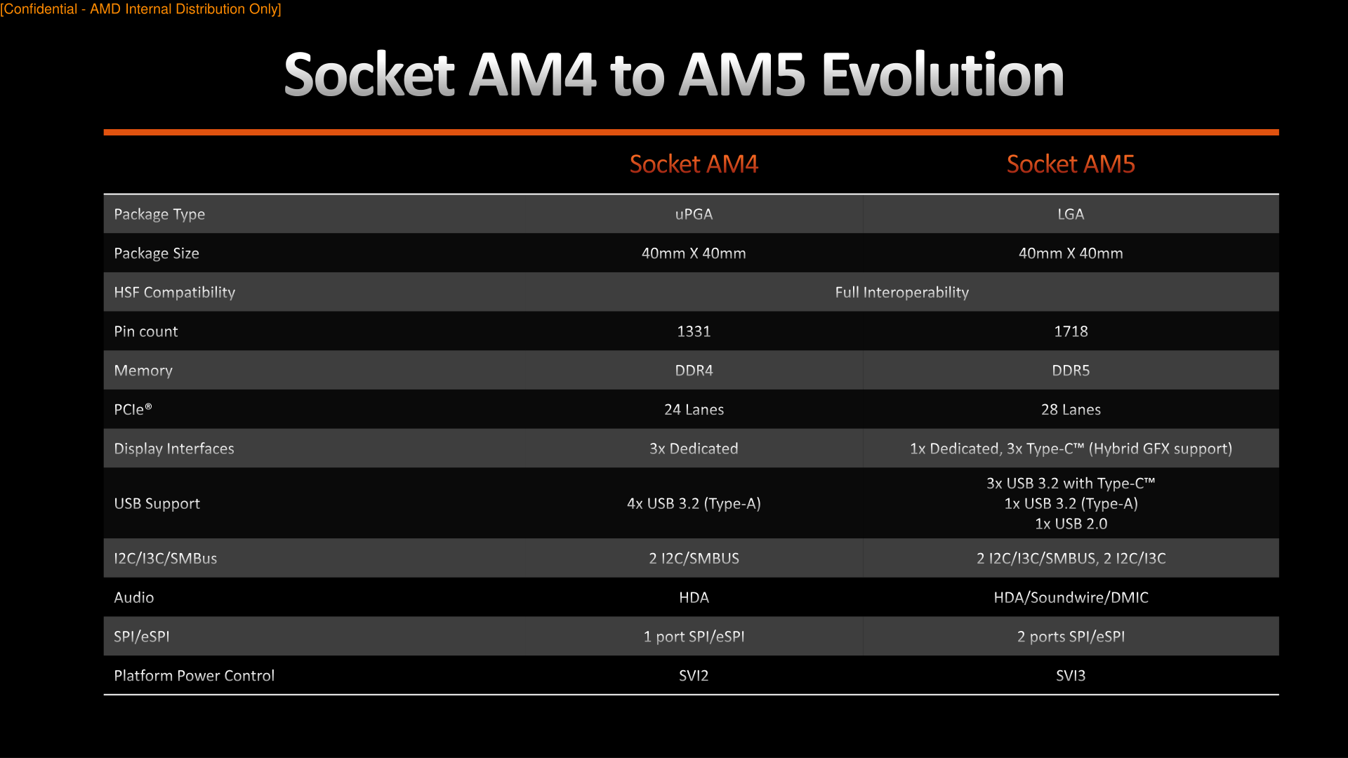
Physically, the most obvious change is of course the socket itself. AMD held on to using pin grid array (PGA) sockets for its mainstream consumer platforms for over a decade after Intel made the switch to land grid array (LGA), but now with AM5 the company is making the switch as well.
As was the case when Intel switched, the shift to LGA brings a couple of benefits, and a couple of trade-offs. Overall LGA allows for greater pin density; whereas socket AM4 was 1331 pins, socket AM5 is 1718 pins in the same package size. This switch also means that the relatively vulnerable pins are moved from the CPU package to the motherboard, which is modestly safer overall. The good news is that this means the days of trying to fix pins on an AMD CPU with a mechanical pencil are coming to an end; the bad news is that if LGA pins are damaged, the motherboard is essentially done for.
This also means that AM5 gets the vastly improved retention mechanisms required by LGA setups, as opposed to the zero-insertion force (ZIF) sockets of the last 30+ years. So CPUs are now much more securely locked down into their sockets, and the errant cases where trying to pull off a cooler and having the CPU come with it is no longer a possibility.
It’s notable here that AMD’s new socket actually has slightly more pins than Intel’s current LGA-1700 socket, at 1718 vs. 1700. Though sharp-eyed power users will note that Intel and AMD have pretty distinct pin configurations (never mind package sizes), with Intel reserving a decent amount of the of the pin pad for placing capacitors and other electronics on the underside of the CPU package, whereas AMD has placed everything on top.
But despite the significant changes in CPU sockets, AMD has worked to preserve backwards compatibility with standard socket AM4 coolers. This is part of the reason for AM5 chips’ odd heatspreader layout, and while I have some personal misgivings about keeping the clips around, there’s no arguing that it will help get the AM5 ecosystem immediately bootstrapped, as it won’t require entirely new coolers. With that said, this compatibility does not extend to coolers that need to replace the stock AMD backplate, so the compatibility rate is not 100%. Builders looking to reuse an old cooler in a system upgrade will want to look into matters to make sure that their cooler is indeed compatible with AM5.
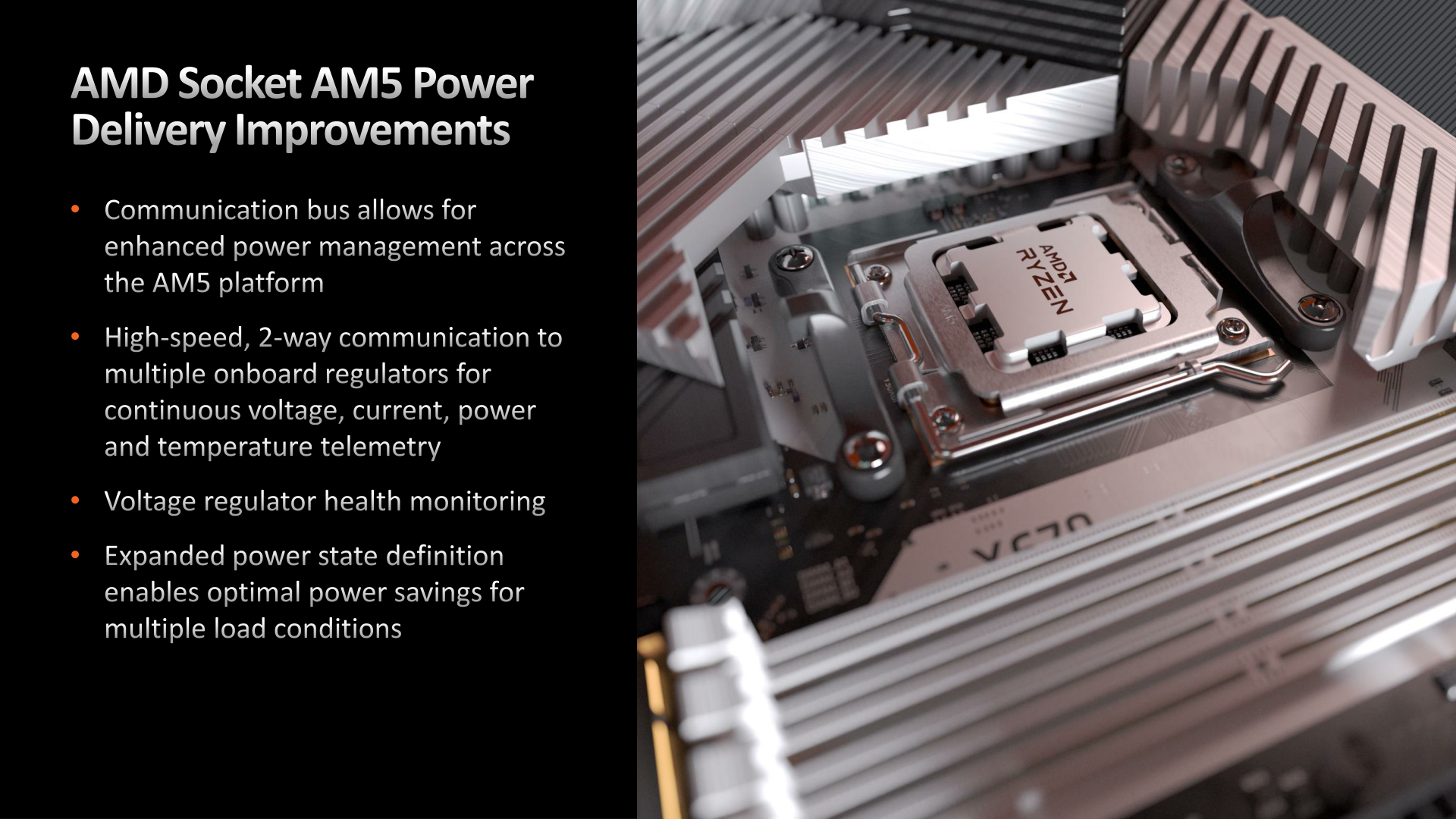
AM5 Power Delivery: Higher Limits & SVI3 Power Management
A big portion of AMD’s new pin budget for AM5 has, in turn, been invested into power delivery. The AM4 platform was designed for CPUs at TDPs up to 105W – or more specifically, a maximum socket power of 142W. As seasoned overclockers already know, this isn’t a hard limit and it’s long been possible to drive more power than this through AM4. But doing so does exceed the design parameters of the socket, the trade-offs of which aren’t advisable for commercial off-the-shelf systems that may need to be supported for several years.
So for AM5, AMD has significantly increased the maximum power they can drive through their socket. The official TDP limit is 170 Watts, which maps out to a total socket power of 230 Watts, a 62% increase in stock power limits. And AMD is going to be taking full advantage of these higher power limits right out of the gate, with the Ryzen 9 7950X and other high-end processors slated to ship with 170W TDPs. In fact this is where a significant chunk of the multi-threaded performance gains from the new Ryzen chips are coming from, as previously AMD’s highest core count CPUs were TDP-constrained when trying to light up all of those cores.
| Stock AMD Socket AM5 TDP Groups | |||||
| 65W TDP | 105W TDP | 170W TDP | |||
| Socket Power (PPT) Watts | 88W | 142W | 230W | ||
| Peak Current (EDC) Amps | 150A | 170A | 225S | ||
| Sustained Current (TDC) Amps | 75A | 110A | 160A | ||
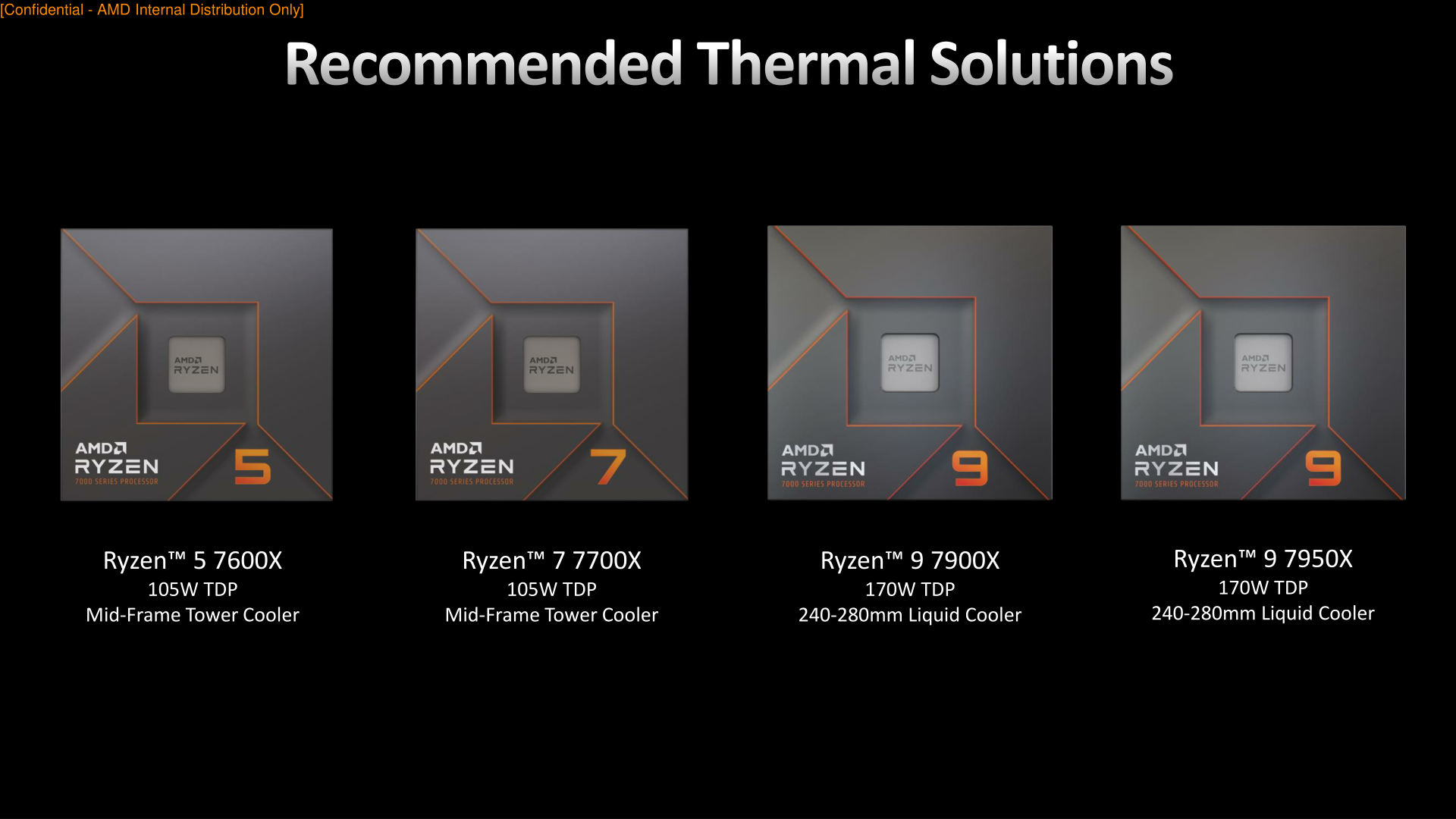
Do note that this also means that cooling requirements are going up. For their 2 CCD parts with 170W TDPs, the 7900X and 7950X, AMD is outright recommending a 240mm (or larger) AIO cooler for keeping those chips under control. AMD only suggests tower coolers for the 1 CCD parts, as these have the same 105W TDP as AMD's former top-end AM4 parts. With that said, this doesn't mean an air cooled setup isn't going to be viable with the higher TDP parts, but you will definitely need a good air cooler if you want to keep ahead on dissipating all of the heat a fully loaded 16C processor can produce.
And while AMD’s peak power consumption is going higher, AMD is also implementing additional technologies to better manage power consumption, and to keep their chips from fully ramping up unless they need to. The big change here is that AMD has ported a lot of their power savings technologies from the Ryzen 6000 Mobile family over to the AM5 platform (and Ryzen 7000 IOD), most notably Scalable Voltage Interface 3 (SVI3), which as in the case of the mobile parts, is designed to allow faster and more discrete control over the voltage required from the chip.
SVI3 is a high-speed, 2-way communications protocol between the CPU and the voltage regulators, allowing the CPU to not only better direct the increasingly large number of VRM phases on high-end motherboards, but to keep an eye on VRM health, monitoring things such as power delivery and VRM temperature. This allows an AM5 CPU to make better and more aggressive decisions about power management, as opposed to having to make more conservative assumptions about the state of the VRMs.
Of particular note here, these upgrades allow for a larger number of overall power states the CPU can be in, which in turn allows for more optimal use of the VRMs. For example, this allows automatic phase shedding to shut off some of the VRM phases feeding the CPU when they’re not needed, which boosts the overall power efficiency of the system (extra phases are great when you need a lot of power, but waste power themselves at low loads).
Altogether, AM5 supplies CPUs with 3 variable power rails, which is up from the 2 rails supplied by AM4. The CPU cores and graphics cores get a shared rail, and there’s a separate SoC rail to power most of the rest of the IOD. Finally, there’s a miscellaneous VDD rail that provides power to the GMI/Infinity Fabric interconnects, along with some other, smaller IPs. Separate from that, there are still fixed rails for things like the memory, 3.3v rail, etc.
Native BIOS Flashback Support
With AMD slated to support the AM5 platform through at least 2025, this time around the company is more actively planning around the future of the platform. In particular, AMD is taking a stab at motherboard forward compatibility, which was increasingly an issue for AM4 over its six-year reign.
The big breaker there was that, even when supported by the chipset, older boards required newer BIOSes to support newer generations of CPUs. Thus the only way to make an old board work with a newer CPU was to flash it with a newer BIOS, which in turn required a working CPU to begin with – a catch 22 situation that ultimately resulted in AMD developing a loaner kit program which rented out older AM4 CPUs that customers could use to flash their older boards if they didn’t already have a new CPU for it (e.g. they just bought it off the shelf).
Ultimately, the more elegant solution to the problem is to allow BIOS flashing without a working CPU (or BIOS), which does an end-run around the whole problem. That exists today in the form of USB BIOS Flashback features; however flashback has been a motherboard-level feature that’s normally only found on select high-end motherboards and has to be implemented by the motherboard vendor itself. So for the AM4 generation, it was not a universal (or even widely available) option.
For the AM5 platform, AMD is taking matters into their own hands to make USB BIOS Flashback a universal feature. Ryzen 7000 chips will be able to support USB BIOS Flashback mode across the board and regardless of the BIOS currently installed. As a result, users will always be able to flash an updated BIOS to their AM5 boards, regardless of the CPUs supported by or the operational status of the current motherboard.
The net impact is that when AMD releases future chips on the AM5 platform – say, a Zen 5 chip in 2024 – it will be possible to install a compatible BIOS without first having to use a Zen 4 chip. Though this does assume, of course, that Zen 5 chips will work in current X/B-600 series boards, which is likely but should not be taken as a given. Otherwise, this change also offers a moderate improvement to the reliability of the AM5 platform, by making it so that the BIOS on any board can be restored should it end up corrupted for whatever reason.
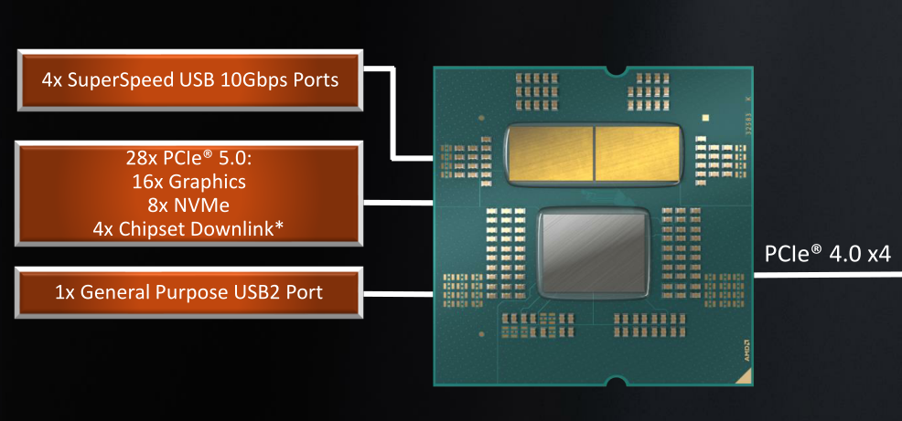
AMD’s other big expenditure using socket AM5’s additional pins is on I/O support. While AM4 already supported a fair bit of I/O, including 24 PCIe lanes, 3 displays, and 4 Superspeed USB ports, there was still room for improvement. So for AM5, AMD has increased the amount of I/O and the flexibility offered with the platform.
The biggest change here is that the AM5 socket now provides for 28 lanes of PCIe, a net gain of 4 lanes. More significantly still, PCIe 5.0 is now supported (at least on the Ryzen 7000 “Raphael” processors), doubling the bandwidth of all of those PCIe lanes to a max of 4GB/sec/lane. Which gives the chip a maximum cumulative PCIe bandwidth of 112GB/sec in each direction.
In practice, those additional lanes are intended for NVMe drives, giving AM5 a second x4 connection to drive a second NVMe drive; though we have seen some motherboard designs where vendors are stealing the second x4 for a PCIe 5.0 x4 slot. Past that, things look a lot like AM4, with 16 PCIe lanes to directly drive one or more PCIe slots, and then 4 lanes for hooking up the chipset.
Meanwhile, the updated socket also offers enough pins for the CPU to drive 4 Superspeed USB 3.x ports, and a USB 2 port. The USB 2 port is new for this generation, and meanwhile 3 of those USB 3 ports now also support the USB Type-C connector, unlike AM4 which could only natively drive Type-A ports. As a result, AM5 CPUs can drive a total of 3 Superspeed Type-C ports, a fourth Superspeed Type-A port, and then the aforementioned USB 2 port.
There has been one regression, however, and that is SATA support. Whereas AM4 CPUs could drive a mix of NVMe and SATA drives (up to 2 SATA + a PCIe x2 for NVMe), AM5 is purely PCIe. So there is no native SATA support on the CPU, and supplying that will come from the chipset.
To visualize this, we’ll use part of the AM5 chipset diagram. We’ll go more into the specifics of the chipsets in a bit, but lays out what is wired to the CPU, and what will need to be wired to the chipset. Of note there, the current chipsets only use PCIe 4.0 connectivity to the Ryzen CPU, so the current generation of chipsets will not be making full use of the bandwidth capabilities of the CPU itself.
Which with the addition of PCIe 5.0 support to the platform, is going to be a recurring theme. While AMD has baked in 5.0 support into the Raphael CPUs, it’s up to motherboard vendors to actually make it so. Compared to PCIe 4.0, 5.0 has much tighter signal integrity requirements (the signaling frequency has been doubled), which at least at this time, makes PCIe 5.0 expensive to implement. A very well-designed motherboard is required with impeccable traces, and on top of that the overall short throw of PCIe 5.0 means that retimers/redrivers become necessary rather quickly. So while AM5 can support PCIe 5.0 throughout, the reality is that we’re still going to see a lot of PCIe 4.0 in use even in higher-end motherboards.
As for the necessity of PCIe 5.0 overall, thus far AMD is primarily focused on what it means for NVMe drive speeds. The first generation of PCIe 5.0-enabled consumer SSDs are expected to land a bit later this year, and they should be able to hit sequential burst transfer rates above the limits of PCIe 4.0 (~7GB/sec).
Past that, NVIDIA’s newly announced Ada Lovelace architecture GeForce RTX 40 series video cards do not support PCIe 5.0. So while we’re awaiting AMD to announce their RDNA 3-based product lineup later this year, regardless of what AMD does, the bulk of video cards sold next year are not going to use PCIe 5.0. So there is a bit less pressure on motherboard manufactures (and motherboard buyers) to get boards that support PCIe 5.0 to anything beyond a couple of M.2 slots.
Finally, in conjunction with the USB I/O changes, AM5 also introduces some display I/O changes. Whereas AM4 could directly drive up to 3 displays, AM5 brings this to 4. Specifically, AM5 offers one dedicated display output (which will generally be allocated to HDMI), while the other 3 display outputs are available over those 3 USB Type-C ports as DisplayPort alt mode. It’ll be up to motherboard manufacturers if they want to expose any of these USB-C root ports as physical USB-C ports or as DisplayPorts, but so far from the motherboard designs we’ve seen, the former is more common (though certainly not universal).
Anticipating a shift to more USB Type-C displays, AMD is also implementing what they call “hybrid graphics” support on AM5. Unlike previous products where this referred to linking up the integrated graphics with a discrete GPU in CrossFire mode, this time around it refers to being able to being able to use the mobo/iGPU’s display outputs to drive a monitor while using a dGPU to render content. This is largely lifted from AMD’s laptop technologies, where similar techniques are used to allow the dGPU to be powered down when it’s not in use. In the case of desktop processors, this just means every display output will work, regardless of whether it’s plugged into ports coming from the CPU or a discrete video card.
It’s also worth noting that AM5 is bringing a few other, more minor updates to other comms protocols. Among these is support for MIPI’s (relatively) new I3C chip-to-chip signaling standard, which will ultimately be supplanting the long-used I2C standard. As well, AM5 doubles the number of I2C/I3C ports available, bringing the total to 4 ports. The platform also adds a second (enhanced) Serial Peripheral Interface (eSPI/SPI) port, and on the audio front, adds support for the Digital Mic and MIPI’s Soundwire standard for low-cost audio peripherals.
Finally, let’s talk about the chipsets that are going to be driving the new AM5 platform. Kicking things off, we have the B650 and X670 chipsets, as well as their Extreme variations. Since AMD is starting the rollout of their new platform with their high-end CPUs, they are matching this with the rollout of their high-end chipsets.
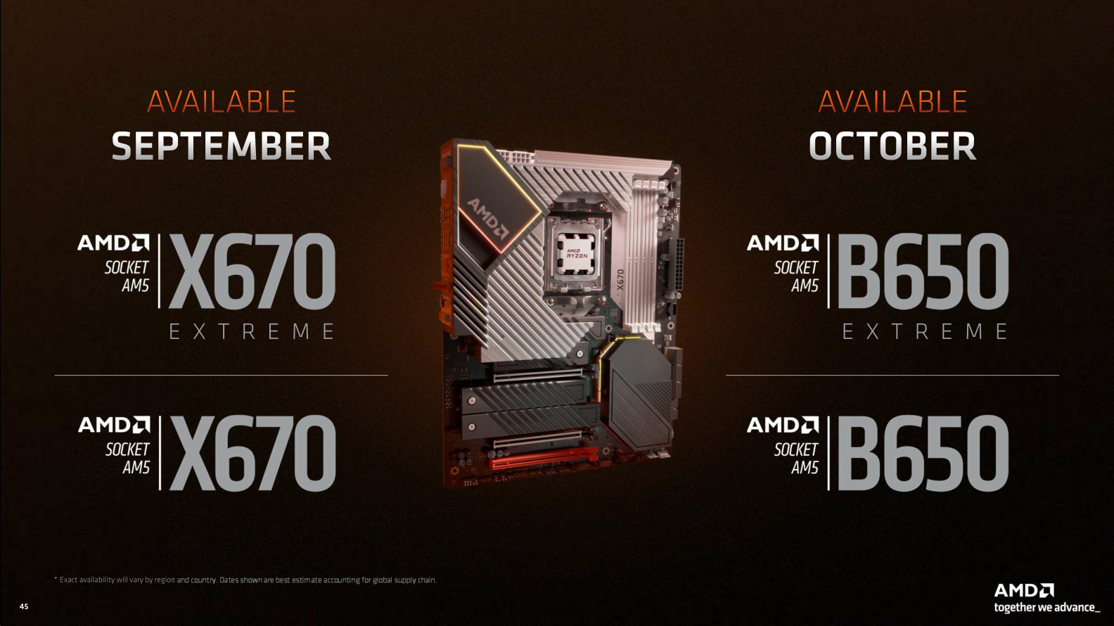
For this week’s launch, the initial boards available are all from the X670 family. B650 boards will, in turn, be coming next month. We’ll break down the difference between the two families below, but at a high level, X670 offers more I/O options than B650. And while not strictly a feature of the chipset, the market segmentation is such that the bulk of high-end AM5 boards – those boards with a massive amount of VRMs and other overclocker/tweaker-friendly features – will be X670 boards.
That said, for simplicity’s sake we’re going to start with the B650 chipset, and build up from there.
| AMD AM5 Chipset Comparison | ||||
| Feature | X670E | X670 | B650E | B650 |
| CPU PCIe (PCIe) | 5.0 (Essentially Mandatory) | 4.0 (5.0 Optional) |
5.0 (Essentially Mandatory) | 4.0 (5.0 Optional) |
| CPU PCIe (M.2 Slots) | At Least 1 PCIe 5.0 Slot | |||
| Total CPU PCIe Lanes | 24 | |||
| Max Chipset PCIe Lanes | 12x 4.0 + 8x 3.0 | 8x 4.0 + 4x 3.0 | ||
| SuperSpeed 10Gbps USB Ports | 4 CPU + 12 Chipset or 4 CPU + 10 Chipset + 1 Chipset 20Gbps or 4 CPU + 8 Chipset + 2 Chipset 20Gbps |
4 CPU + 6 Chipset |
||
| DDR5 Support | Quad Channel (128-bit bus) Speeds TBD |
|||
| Wi-Fi 6E | Yes | |||
| CPU Overclocking Support | Y | Y | Y | Y |
| Memory Overclocking Support | Y | Y | Y | Y |
| Available | September 2022 | October 2022 | ||
B650, AMD’s mainstream AM5 chipset, can best be thought of as a PCIe 4.0 switch with a bunch of additional I/O baked in. And as is typical for chipsets these days, several of the I/O lanes coming from the chipset are flexible lanes that can be reallocated between various protocols. Meanwhile, uplink to the CPU is a PCIe 4.0 x4 connection.
For PCIe connectivity, B650 offers 8 PCIe 4.0 lanes, which can either have PCIe slots or further integrated peripherals (LAN, Wi-Fi, etc) hung off of them. This and the uplink speed are both notable improvements over the B550 chipset, which was PCIe 3.0 throughout, despite Ryzen 3000/5000 offering PCIe 4.0 connectivity. So B650 has a lot more bandwidth coming into it, and available to distribute to peripherals.
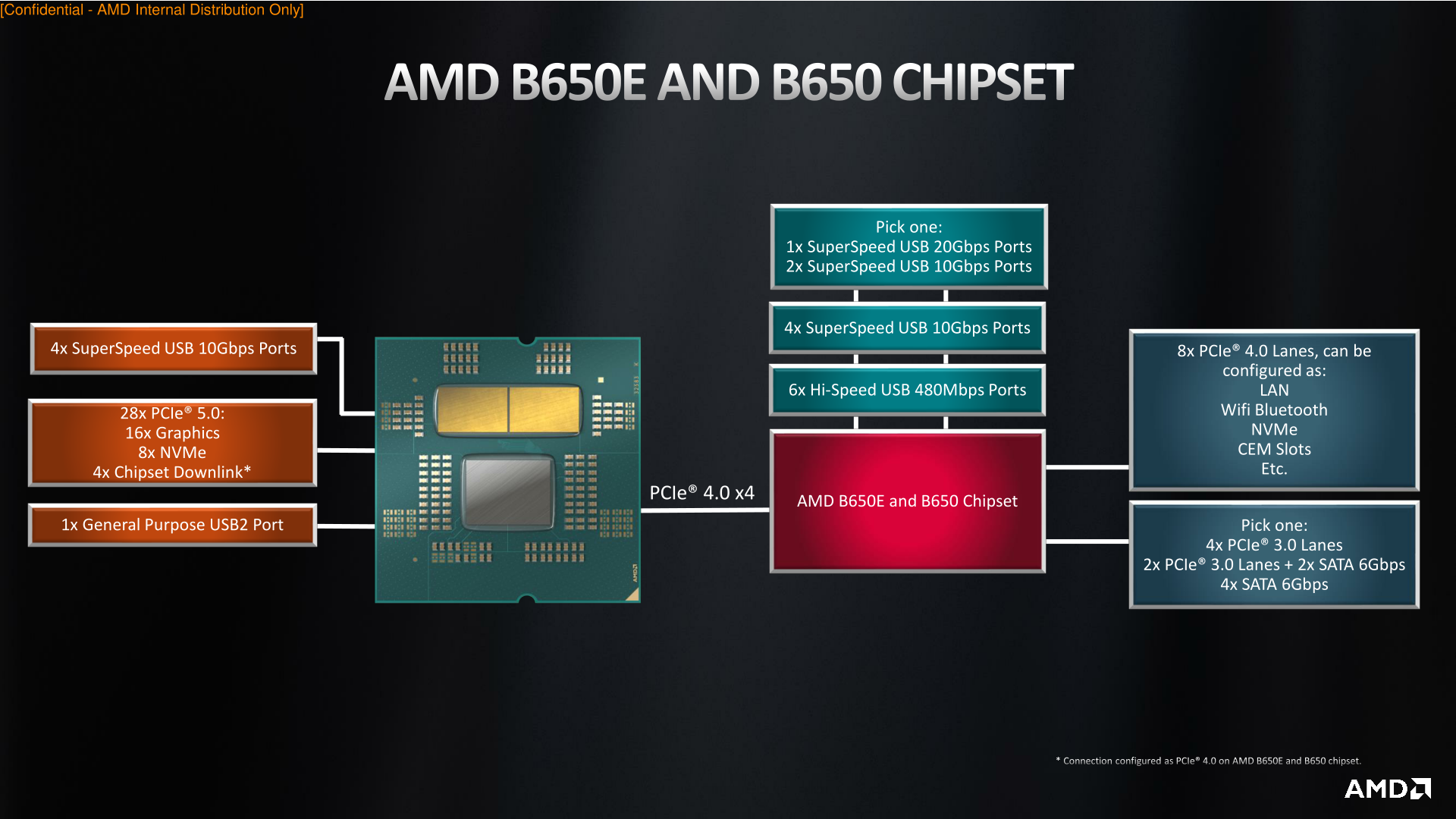
There are also a quartet of PCIe 3.0 lanes which are shared with the SATA ports, allowing for either 4 PCIe lanes, 2 lanes + 2 SATA, or 4 SATA ports. Notably, the dedicated SATA ports found on the 500 series chipsets are gone, so motherboards will always have to sacrifice PCIe lanes to enable SATA ports. For the B650 this amounts to a net loss of 2 SATA ports, as the most ports it can drive without a discrete storage controller is 4.
Meanwhile on the USB front, motherboard vendors get more Superspeed USB ports than before. The chipset offers a fixed 4 10Gbps Superspeed ports, and then an additional output can be configured as either a single 20Gbps (2x2) port, or two 10Gbps ports. Finally, the chipset can drive a further 6 USB 2 ports, mostly for on-board peripheral use. There are no USB root ports limited to 5Gbps here, so all USB 3.x ports, whether coming from the CPU or the chipset, are capable of 10Gbps operation.
AMD has once again outsourced chipset development for this generation to ASMedia, who also designed the B550 chipset. AMD has not disclosed a TDP for the chipset, but like B550 before it, it is designed to run with passive cooling.
Outside of the technical capabilities of the B650 chipset itself, AMD is also imposing some feature requirements on motherboard makers as part of the overall AM5 platform, and this is where the Extreme designation comes in. All B650 (and X670) motherboards must support at least 1 PCIe 5.0 x4 connection for storage; Raphael has enough lanes to drive two storage devices at those speeds, but it will be up to motherboard manufacturers if they want to actually run at those speeds (given the difficulty of PCIe 5.0 routing).
Extreme motherboards, in turn, will also require that PCIe 5.0 is supported to at least one PCIe slot – normally, the x16 PCIe Graphics (PEG) slot. Non-extreme motherboards will not require this, and while motherboard vendors could technically do it anyhow, it would defeat the purpose of (and higher margins afforded by) the Extreme branding. Conversely, while AMD has been careful to toe a line about calling 5.0 slots outright mandatory on Extreme motherboards, it’s clear that there’s some kind of licensing or validation program in place where motherboard makers would be driving up their costs for no good reason if they tried to make an Extreme board without 5.0 slots.
It’s frankly more confusing than it should be, owing to a lack of hard and definite rules set by AMD; but the messaging from AMD is that it shouldn’t be a real issue, and that if you see an Extreme motherboard, it will offer PCIe 5.0 to its graphics slot. Past that, offering 5.0 to additional slots, bifurcation support, etc is up to motherboard vendors. The more PCIe 5.0 slots they enable, the more expensive boards are going to be.
Meanwhile the high-end counterpart to the B650 chipset is the X670 chipset, which is pretty much just two B650 chipsets on a single board. While not explicitly confirmed by AMD, as we’ll see in the logical diagram for X670, there’s no way to escape the conclusion that X670 is just using B650 dies daisy chained off of one another to add more I/O lanes.
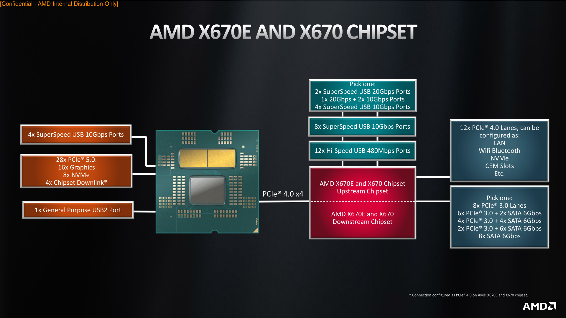
Officially, X670 is a two-chip solution, using what AMD terms the “downstream” and “upstream” chipsets. The upstream chip is connected to the CPU via a PCIe 4.0 x4 connection, and meanwhile the downstream chip is connected to the upstream chip via another PCIe 4.0 x4 connection.
By doubling up on the number of chips on board, the number of I/O lanes and options are virtually doubled. The sum total of the two chips offers up to 12 PCIe 4.0 lanes (the last 4 are consumed by the upstream chip feeding the downstream chip) and a further 8 PCIe 3.0 lanes that can be shifted between PCIe and up to 8 SATA ports.
Meanwhile on the USB front, there are now 8 fixed USB 2 ports and 8 fixed SuperSpeed USB 10Gbps ports. For USB flex I/O, motherboard makers can select from either 2 20Gbps ports, 1 20Gbps port plus 2 10Gbps ports, or 4 10Gbps ports.
And while this configuration adds more I/O lanes (and thus more I/O bandwidth), it should be noted that all of these I/O lanes are still gated behind the PCIe 4.0 x4 connection going back to the CPU. So the amount of backhaul bandwidth available between the chipsets and the CPU is not any higher than it is on B650. The name of the game here is flexibility; AMD is not designing this platform for lots of sustained, high-speed I/O outside of the CPU-connected x16 PCIe graphics slot and M.2 slots. Rather, it’s designed to have a lot of peripherals attached that are either low bandwidth, or only periodically need high bandwidths. If you need significantly more sustained I/O bandwidth, then in AMD’s ecosystem there is a very clear push towards Threadripper Pro products.
Finally, X670 Extreme (X670E) will impose the same PCIe 5.0 requirements as B650E. This means Extreme boards will offer PCIe 5.0 connectivity for at least one PCIe lane, while X670 boards are expected to come with just PCIe 4.0 slots. These will be the most expensive boards, owing to a combination of requiring two chipsets, as well as the extra costs and redrivers that go into extending PCIe 5.0 farther throughout a motherboard.
On that note, when discussing the new chipsets with AMD, the company did offer an explanation for why X670 daisy chains the chipsets. In short, daisy chaining allows for additional routing – the downstream chipset can be placed relative to the upstream chipset, instead of relative to the CPU (and PCIe devices then placed relative to the chipsets). In other words, this allows for spreading out I/O so that it’s not all so close to the CPU, making better use of the full (E)ATX board. As well, hanging both chipsets off of the CPU would consume another 4 PCIe lanes, which AMD would rather see going to additional storage.
The final major feature being introduced with the AM5 platform is DDR5 memory support. Like AM4, which was introduced alongside AMD’s shift over from DDR3 to DDR4, socket AM5 is being rolled out to bring support for DDR5 for the platform.
In fact, socket AM5 only brings DDR5 support. Unlike rival Intel, who opted to support both DDR4 and DDR5 memory with their Alder Lake (12th Gen Core) CPUs, AMD is only supporting DDR5 on the AM5 platform. This is a true platform limitation, and there is no going back.
Like other engineering decisions, this marks a trade-off being made by AMD. In the short term, this is going to drive up the total cost of an AM5 system relative to a theoretical AM5 system with DDR4 memory; DDR5 simply costs more right now. But at the same time, it simplifies things over the long run of the platform, especially since AMD is planning on supporting it through 2025. There will be no such thing as a DDR4 AM5 motherboard, and AMD needs not bake DDR4 support into any of the Ryzen memory controllers.
Ultimately, with AMD starting the DDR5 transition roughly a year after Intel, the company’s expectations are that DDR5 prices are going to continue falling fast enough that they’re going to reach parity with DDR4 before too long. So why implement DDR4 support if it’s only going to be necessary for a short period of time?
As for memory speeds and capacities supported, while AM5 enforces the use of DDR5, ultimately it’s the individual memory controllers that determine the rest. For AMD’s Ryzen 7000 desktop processors, which are based on the Zen 4 Raphael design, these chips offer support for official (JEDEC) speeds at up to DDR5-5200 for a 1 DIMM Per Channel (DPC) configuration. But, like all other DDR5 products we’ve seen thus far, 2 DPC comes with a significant penalty; in that case the maximum JEDEC speed is reduced to just DDR5-3600.
So as was the case with Intel’s Alder Lake platform, system builders are going to need to put a lot more thought into how they go about adding memory, and how they’re going to handle future memory expansion, if at all. While Ryzen 7000 can drive a 2 DPC/4 DIMM setup, you’re going to lose 31% of your memory bandwidth if you go that route. So for peak performance, it’ll be best to treat Ryzen 7000 as a 1 DPC platform.
Meanwhile, for system builders looking at reliability and data integrity as opposed to performance, AMD has confirmed that Ryzen 7000 also supports ECC memory. Unfortunately, the compatibility situation is essentially unchanged from the AM4 platform, which is to say that while the CPU supports ECC memory, it’s going to be up to motherboard manufacturers to properly validate it against their boards. For boards that aren’t doing validation, AMD can’t guarantee ECC is going to work. Though it’s largely a moot point for today’s launch anyhow, since although DDR5 ECC UDIMMs exist, they are in very short supply.
Also, while we didn’t expect it to be supported to begin with, AMD has confirmed that Ryzen 7000 won’t support RDIMMS/LRDIMMs. So it’s unbuffered DIMMs all the way.
Overclocking Memory Ratios
JEDEC standard speeds aside, the Ryzen 7000 series will also support memory overclocking. And thanks to a combination of the switch to DDR5 memory, changes to AMD’s memory controllers, and changes to AMD’s power delivery infrastructure, the rules have changed.
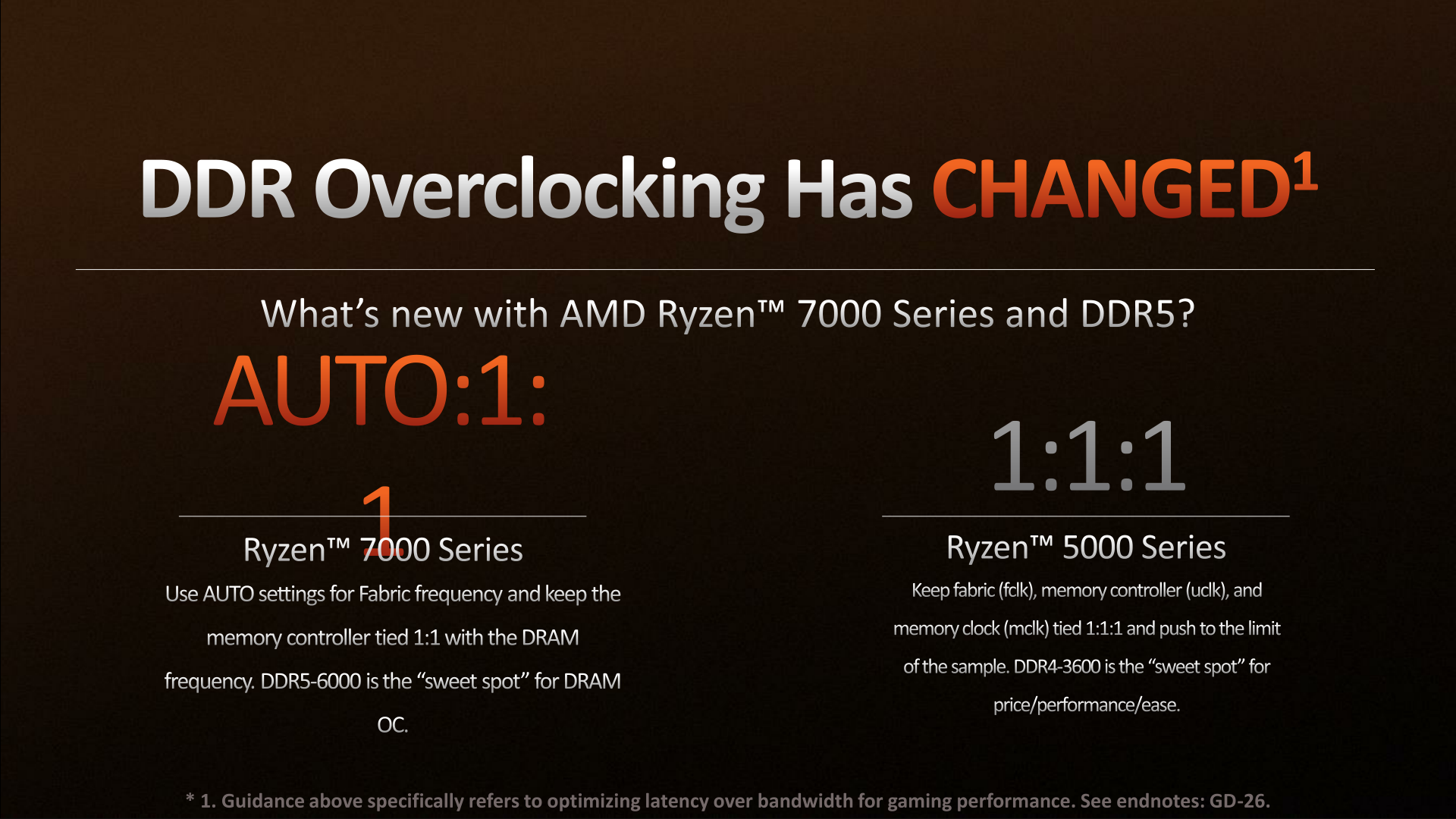
On Ryzen 5000, the ideal configuration for memory overclocking was to run the fabric clock, memory controller, and memory clock all in sync at the same frequencies. This made DDR4-3600 the typical “sweet spot” for the platform, as going faster would typically require running parts of the CPU out of sync so that they could stay within their own attainable clockspeeds.
But for Ryzen 7000, AMD has loosened things up a bit. Ryzen 7000 systems can still get improved memory performance even when the fabric clock is allowed to go out of sync with the memory controller. As a result, most overclockers can just leave that clock set to Auto, and instead focus on keeping the memory and memory controller clocks in sync in a 1:1 ratio.
Specifically, when the fabric clock is set to Auto, it’s typically run at 2000MHz. Meanwhile the memory and memory controller clocks will be running at anywhere between 2400MHz and 3000MHz, depending on the speed of the RAM kit used. Ultimately, the goal for the best performance is to get the fabric clock to 2000MHz and then keep the memory/MC clock at 3000MHz or less. Otherwise, if memory speeds exceed 3000MHz (DDR5-6000), then the memory controller will fall to 1:2 with the memory frequency, which will incur a performance hit.
It should be noted that AMD’s idea of optimal memory speeds here is high memory clocks with low memory latencies, rather than pushing the absolute fastest memory clocks. On good chips it should be possible to drive Ryzen 7000 at speeds above DDR5-6000, but the latency hit from things falling out of sync will be significant – enough so that it’s likely going to be a performance regression for most workloads.
Overclocking with EXPO
But for most users doing memory overclocking, they’re likely going to simply rely on factory overclocked memory kits with pre-programmed profiles. And this is where AMD is rolling out their own standard for those memory kit profiles: EXPO.
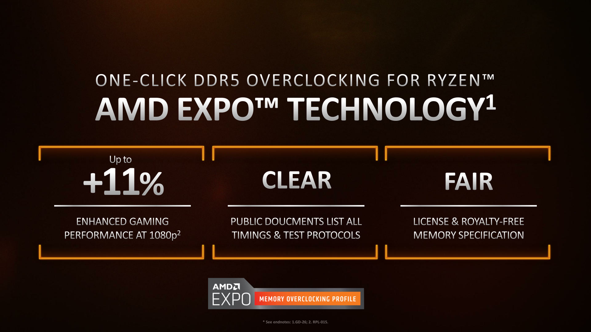
AMD EXPO stands for EXtended Profiles for Overclocking and is designed to provide users with high-end memory overclocking when used in conjunction with AMD's Ryzen 7000 series processors. Similar to Intel's preexisting X.M.P (Extreme Memory Profile) technology found on most consumer-level memory kits designed for desktop Intel platforms, AMD's EXPO technology aims to do the same, but as an open standard with an emphasis on providing the best settings for AMD platforms.
The premise of AMD EXPO is that is a one-click DDR5 overclocking function for AM5 motherboards. On the surface EXPO is essentially a set of X.M.P-like profile specifically designed for AMD's Ryzen 7000 (Zen 4) processors.
The major impetus behind EXPO is two-fold. The first is simple: Intel doesn’t share XMP. There’s no published specification for it, and while AMD has reverse engineered it to some extent, they can’t be sure of what’s going on (especially with DDR5/XMP 3). So rather than deal with the potential compatibility issues and inefficiencies, they’re just going their own way. The second benefit for EXPO being that it means that memory kit manufacturers can then create memory profiles that are AMD-specific, potentially using tighter sub-timings that are possible in conjunction with AMD processors, but not with Intel’s.
It is worth noting that, despite the existence of EXPO, DDR5 memory with X.M.P profiles will be supported on Ryzen 7000 platforms. Still, AMD is very clearly pushing customers towards using EXPO DIMMs with their systems to get the best performance out of AMD systems.
As for EXPO itself, like most other AMD standards, the company is making this an open and royalty free standard (XMP is believed to have royalties, but how much has never been officially published). So memory kit partners will be able to implement EXPO profiles without the blessing of AMD, or needing to pay AMD for the privilege.
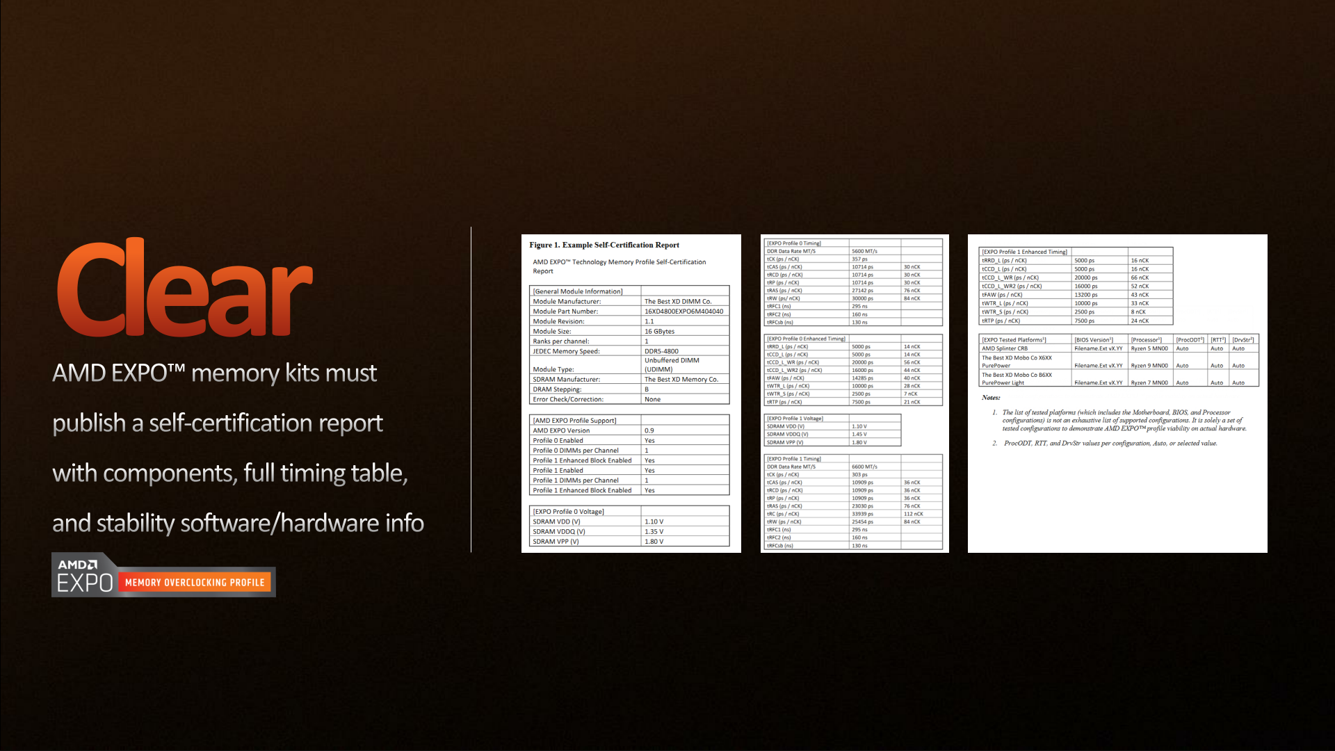
With that said, EXPO will be a self-certification program. So AMD is not charging anything for it, but at the same time they are not doing much in the way of extra work to validate support for it.
In lieu of that, memory kit manufacturers will be required to publish their self-certification reports. These reports will lay out in detail what memory was tested on what systems, and with what timings and voltages. The idea here being that openness goes both ways, and that buyers should be able to see complete configuration settings a profile calls for. The detailed data is in some respects overkill, but it also means that if memory kit manufacturers opt for a high-clocked kit with tight primary timings and loose secondary timings, potential customers will be able to see those full timings in advance.
As with manual memory overclocking, AMD expects the sweet spot for EXPO kits to be DDR5-6000. In an example profile provided for a 2 x 16GB G.Skill memory kit, that kit runs at DDR5-6000 CL30, with a VDD voltage of 1.35v. It’s kits like these that AMD expects to provide the best performance, offering rather low memory latencies in conjunction with a more modest increase in memory frequency.
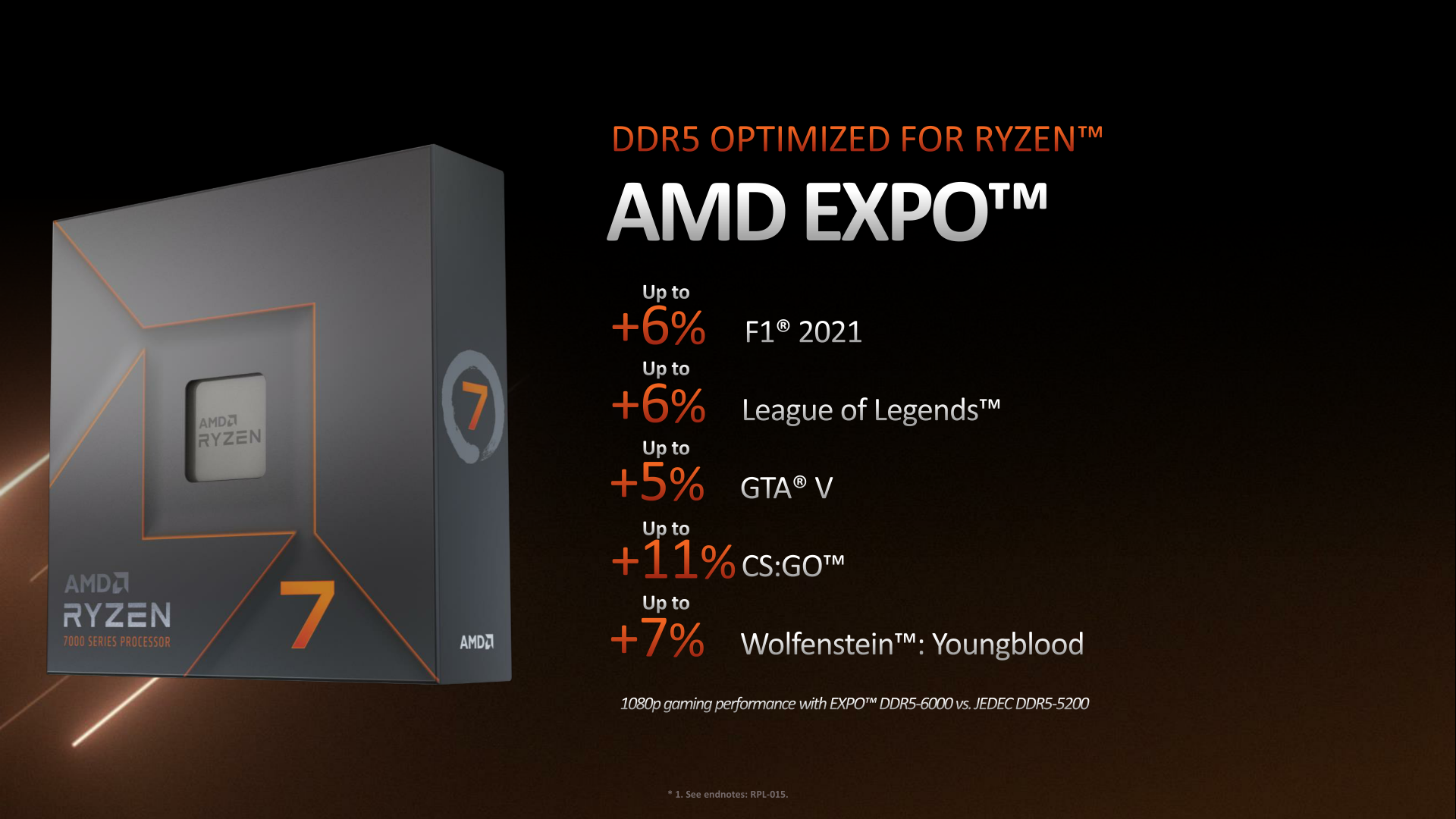
The specific performance gains will vary depending on the workloads. But for gaming tasks, some of the most DRAM latency-sensitive workloads, AMD is touting performance gains of up to 11% at 1080p. Otherwise, at more GPU-limited resolutions and settings, the gains will be understandably lower.
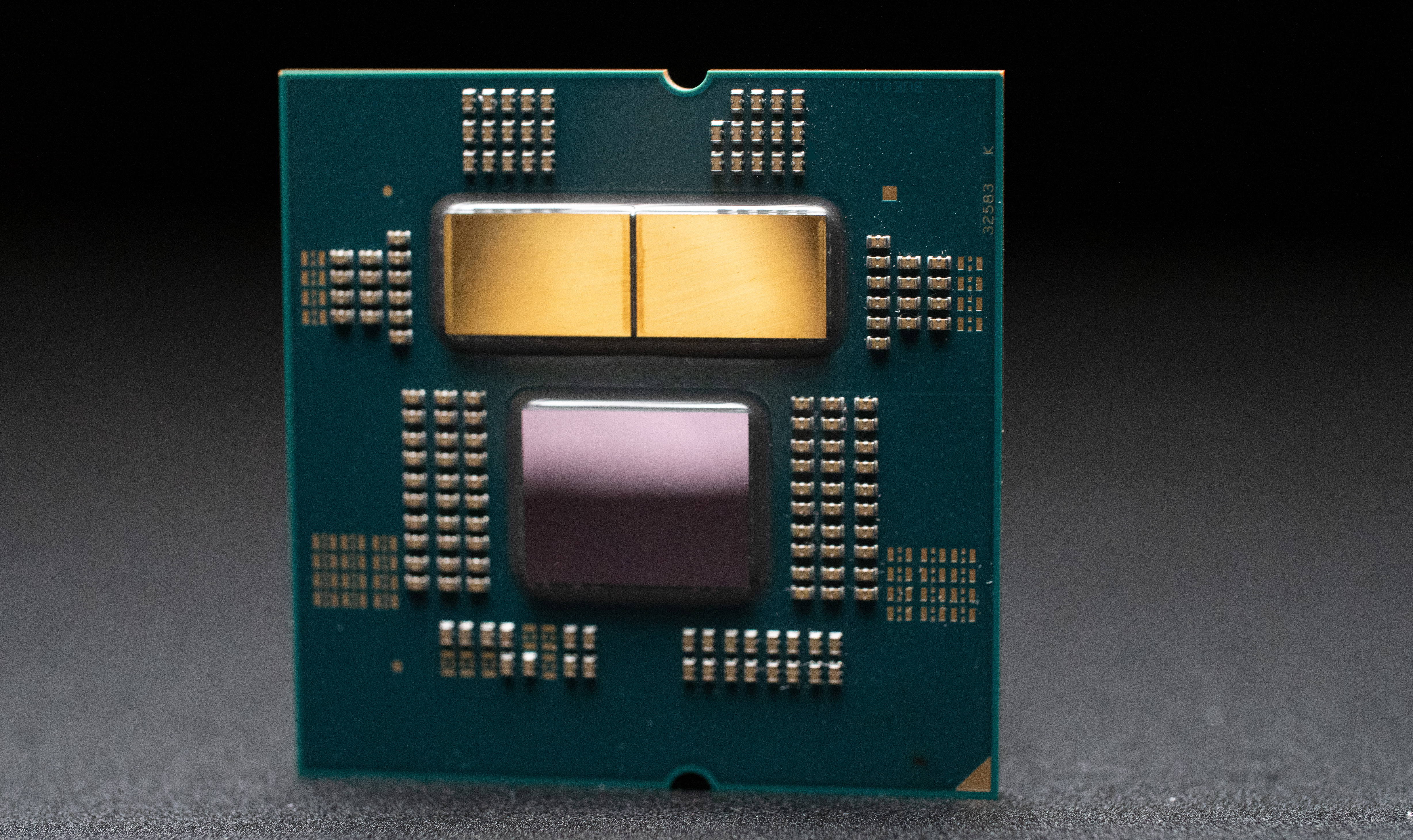
We’ll start our look at the Ryzen 7000 silicon with the glue that holds the chip together: the I/O Die (IOD). Whether it’s a 7600X or 7950X – one CPU chiplet or two – every Ryzen 7000 processor gets one of AMD’s new IODs.
As with the Ryzen 3000/5000 series, the IOD is a die separate from the CPU core chiplets that hosts everything that isn’t the CPU cores or their associated L1/L2/L3 caches. By producing a 2 or 3 chiplet-based solution rather than a single monolithic die, AMD is able to put silicon that doesn’t require cutting-edge performance on a cheaper process node, while enjoying the yield advantages that come from smaller chiplets and older, more mature nodes.
And yet with that said, for the Ryzen 7000 series it’s AMD’s IOD that’s getting the biggest upgrade. Previously produced on GlobalFoundries’ 14nm/12nm process node, for Ryzen 7000 the IOD has made the leap to TSMC. The new IOD is made on TSMC’s 6nm process, a generation behind the 5nm node used for the CPU chiplets themselves, but a generation (and then-some) ahead of GlobalFoundries’ smallest node.
With AMD no longer tightly bound to GloFo with wafer share agreement exclusivity requirements, AMD is now free to produce chips like the IOD where they see fit. And with AMD also doing very well as a company in the last few years, they do not need to produce IODs at GloFo to meet their purchase requirements with the fab.
The jump to TSMC 6nm brings several advantages to AMD’s central chiplet. The much smaller process node allows for significantly more transistors – 3.4B on a 122m2 die, 63% more than before – which AMD can invest in new features such as integrated graphics. As well, the more efficient process node brings down the power requirements of the IOD, especially in near-idle situations, though AMD is relying on a lot more than process nodes here.
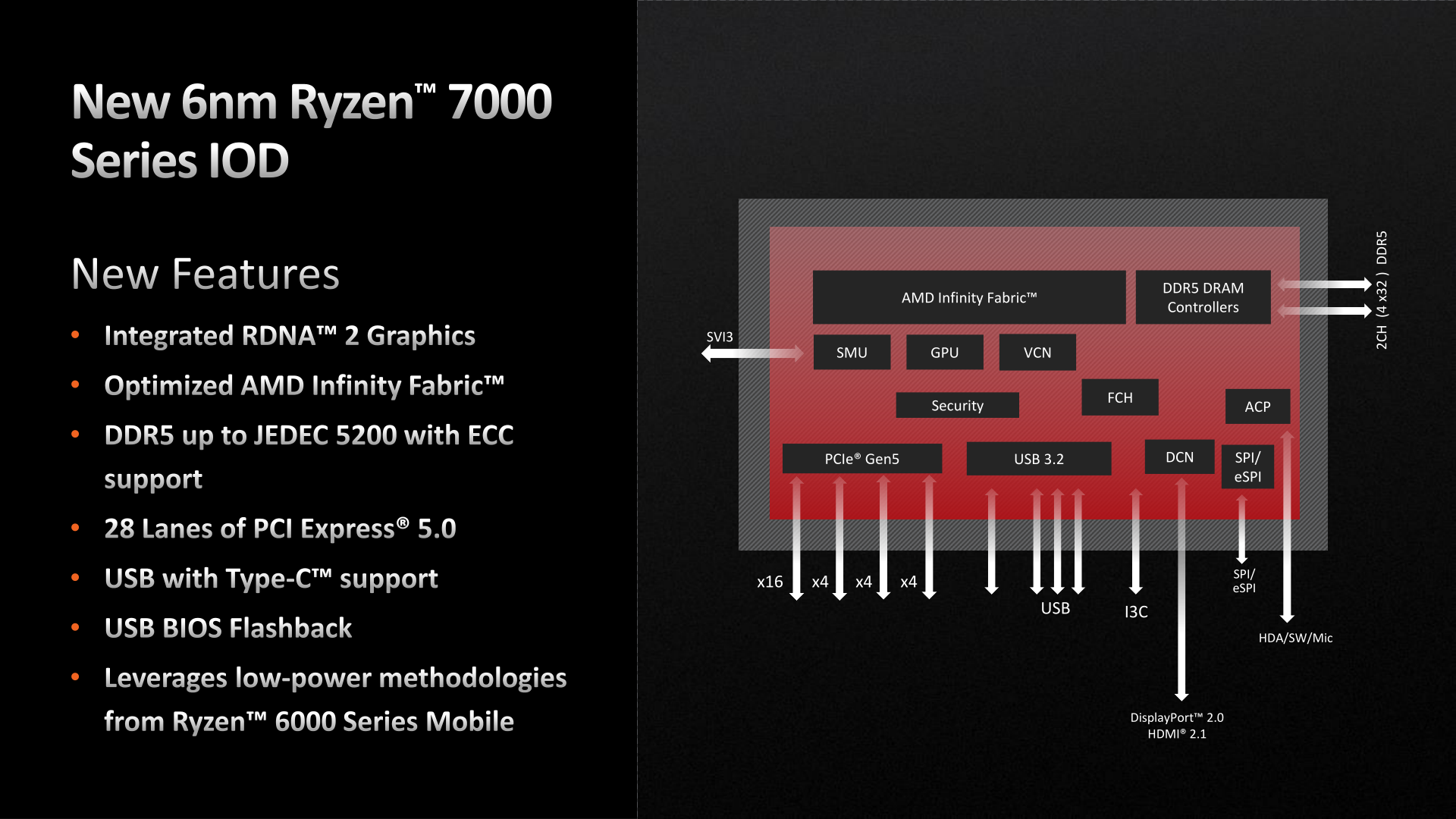
In terms of functionality, the IOD first and foremost is responsible for the CPU-side implementation of all the new features of the AM5 platform. So PCIe 5.0 root complexes, DDR5 memory support, updated display I/O, and more are implemented here. Relative to the Ryzen 3000/5000 IOD then, there is almost nothing here that AMD hasn’t touched in some function; even the USB controllers and infinity fabric have been altered for this generation of processors.
Ryzen 6000 Mobile’s Legacy: Power Control and Pluton
Outside of the obvious gains from moving to a smaller process node, the Ryzen 7000 IOD has also given AMD a chance to implement everything they’ve learned in the past 3 years about power control and power optimizations from the Ryzen mobile lineup. Since the previous-generation IOD was launched for the Ryzen 3000 family in 2019, AMD has launched the Ryzen 6000 Mobile CPU, a monolithic die design that went all-out on power efficiency improvements in a bid to catch up to Intel. Ryzen 6000 Mobile introduced power features such as SVI3, which have since been ported to the Ryzen 7000 design, and principally show up as parts of the IOD.
This was especially easy for AMD as the IOD is made on the same 6nm process as the Ryzen 6000 Mobile chips. Which means that the new IOD has been able to implement many of the same power gating, power binning, deep sleep modes, clock gating, and power state features that were first introduced for mobile. Which is to say that AMD has put a lot of hard work into keeping the IOD from working hard.
The Ryzen 7000 also inherits many of the basic security features of the Ryzen 6000 Mobile platform. AMD is still using their own Arm-based security processor within the IOD. And the new chip is compliant with Microsoft’s Pluton initiative as well – with all the mixed responses that will undoubtedly come from that.
Ryzen 7000 Becomes Whole: Integrated Graphics At Last
Of the additional 1.31B transistors in AMD’s new IOD, the single biggest spend against that budget comes from the long-awaited inclusion of integrated graphics on high-end Ryzen desktop parts. Up to this point, AMD’s high-end consumer Ryzen processors have not included integrated graphics; both the early monolithic parts and later chiplet-style parts have forgone them for cost and integration reasons. But now with AMD’s modern RDNA 2 graphics architecture and TSMC fabrication process, AMD has finally seen the (ray traced) light, and is building a small GPU block into the IOD to offer integrated graphics throughout the Ryzen 7000 product stack.
To be sure, this iGPU is not a very powerful one – and it’s not meant to be. With just 2 CUs (technically a single RDNA 2 dual compute unit), it offers one-sixth the number of CUs on AMD’s top-end Ryzen Mobile APUs, or in the bottom-of-the-stack discrete Radeon RX 6400. So this is not a configuration meant to replace AMD’s traditional APUs in laptop or desktop scenarios. None the less, it is a full implementation of the RDNA 2 architecture – ray tracing and all – in a very low performance configuration.
| AMD GPU Specificaiton Comparison | |||||
| AMD Radeon Graphics (Raphael) |
AMD Radeon 680M (Rembrandt) |
AMD Radeon RX 6400 | |||
| Stream Processors | 128 (2 CUs) |
768 (12 CUs) |
768 (12 CUs) |
||
| Boost Clock | 2200MHz | 2400MHz | 2321MHz | ||
| Peak Throughput (FP32) | 0.56 TFLOPS | 3.7 TFLOPS | 3.6 TFLOPS | ||
| Memory Clock | DDR5-5200 | LPDDR5-6400 | 16 Gbps GDDR6 | ||
| Memory Bus Width | 128-bit | 128-bit | 64-bit | ||
| Infinity Cache | N/A | N/A | 16MB | ||
| Manufacturing Process | TSMC N6 | TSMC N6 | TSMC N6 | ||
| Transistor Count | N/A | N/A | 5.4B | ||
| Architecture | RDNA2 | RDNA2 | RDNA2 | ||
| GPU | Raphael Integrated | Rembrandt Integrated | Navi 24 | ||
The idea behind including an iGPU here is to offer a basic implementation of modern graphics across the entire Ryzen 7000 lineup. Even though it’s not very fast, 2 CUs running at up to 2.2GHz is going to be fast enough for desktop work – and maybe even some very light gaming. This makes the high-end Ryzen chips suitable for desktop work and inclusion in OEM desktop systems without a discrete GPU, a market segment that AMD was previously locked out of and Intel enjoyed free reign. And even for users who are bringing their own GPU, an integrated GPU makes troubleshooting all the easier, as now it doesn’t require a separate video card to merely boot a system.
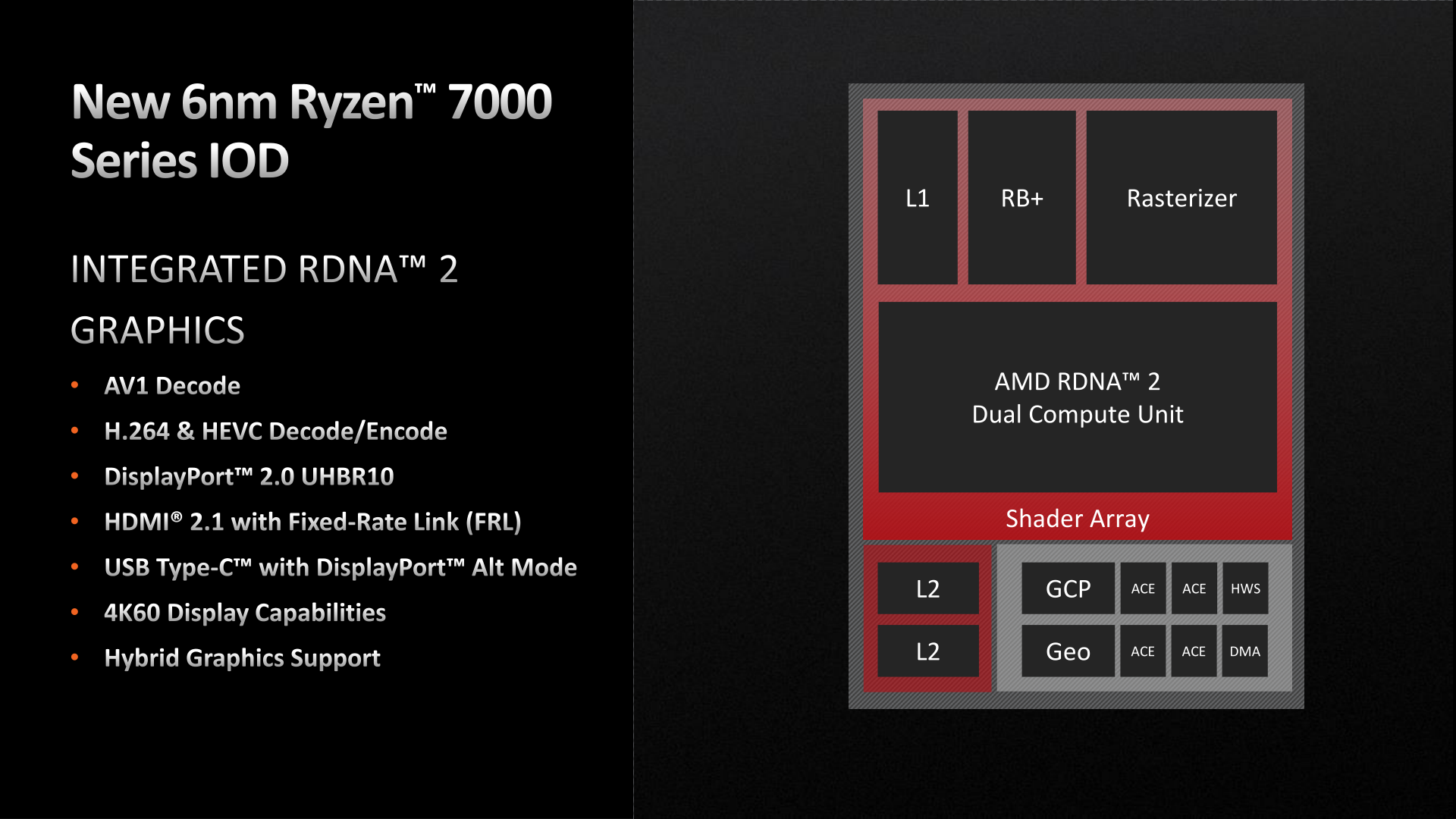
Besides enabling basic pixel processing, the other major function of the Ryzen 7000 iGPU is to enable all of the video decoding and video output functionality expected from a modern GPU. As this part is derived from the integrated GPU that when into Ryzen 6000 Mobile (Rembrandt), it comes with a very familiar feature set. That includes AV1, HEVC, and H.264 video decoding, as well as HEVC and H.264 video encoding. And, as AMD is keen to point out, these video encode/decode blocks remain accessible even with a discrete GPU in play; so unless a user outright disables the iGPU, every Ryzen 7000 system will have access to a modern suite of video encode and decode features.
Meanwhile on the display controller side of matters, this is the block that’s enabling Ryzen 7000 CPUs to drive up to 4 4K@60Hz displays. The iGPU display controllers can drive HDMI 2.1 up to its maximum 48Gbps data rate, or it can drive a DisplayPort 2.0 output at up to the UHBR10 data rate (a feature not even found on NVIDIA’s forthcoming RTX 40 series cards). And as mentioned previously when talking about motherboards and chipsets, motherboard vendors will have the option of exposing these DP outputs either via USB-C alt mode, or by implementing fixed DisplayPorts. All of which, in turn, can be used as active display outputs even if a discrete video card is installed, via AMD’s new hybrid graphics mode.
All told, AMD is taking a similar tack as Intel here with their desktop CPUs. Most (but not all) Intel desktop parts contain a basic UHD-class integrated Xe-LP GPU, which Intel does for many of the same reasons as AMD now is. AMD has a leg-up on Intel in as much as they offer a newer architecture and features to much, such as AV1 decoding. But we’ll have to see where performance lands; 2 Radeon CUs is low enough that these parts may not even catch up to Intel’s 32 EU integrated graphics.
AMD Infinity Fabric: Faster Flowing, Narrower Going
The last major functional update to come with AMD new IOD is the Infinity Fabric, AMD’s die-to-die interconnect. On the chiplet-based Ryzen desktop parts, IF is used to provide a low-latency connection between the IOD and the CPU core chiplet(s) on the package.
For the Ryzen 7000 series, AMD has done some further engineering work to reduce the power costs of the IF links, and thus improve the overall power efficiency of the link and reduce the data movement power penalty for using a chiplet-based approached. The most significant thing here is that AMD has doubled the IF link frequency, but cut the physical width of the IF link in half. As a result, Ryzen 7000’s IF links offer the same bandwidth as on Ryzen 5000,
According to AMD, this refactoring is because AMD’s engineers found that, contrary to conventional wisdom, they could save power running a narrower IF link at a higher frequency. Which is to say that, even though higher frequencies are normally power prohibitive, in the case of IF it’s just powering the physical links themselves which is the most expensive part. Part of that shift, in turn, comes from the fact that the newer process nodes have allowed AMD to run the IF link at a lower voltage,
Finally, further reducing AMD’s power consumption here, the IF links on the Ryzen 7000 now support multiple power states, versus the binary on/off states of the IF links on Ryzen 5000 and earlier. This gives AMD a nice middle ground to save power in lighter load situations, by being able to use intermediate states rather than running at full-power just to have an IF link active.
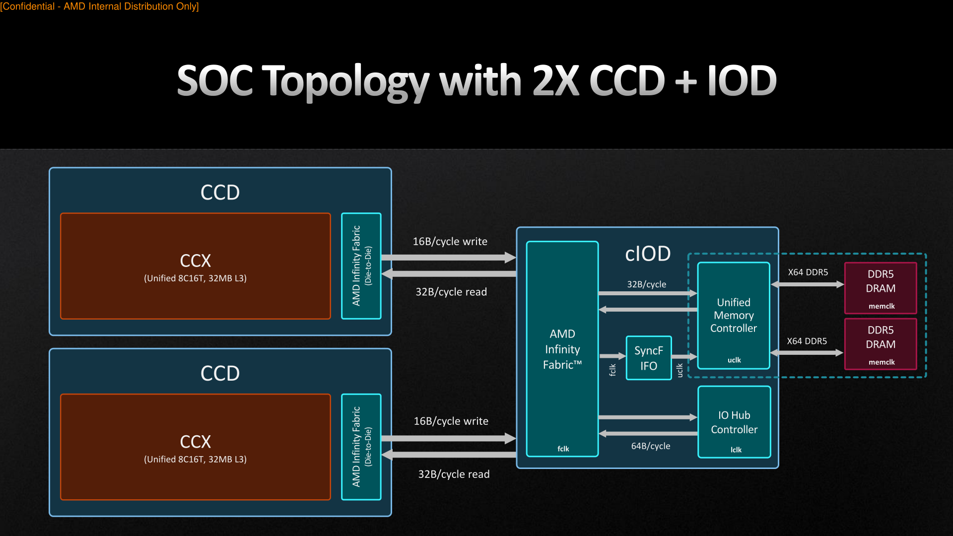
And while this leaves AMD with an obvious (if more power-hungry) route to take for more IF bandwidth in the future should they need it, for now the company intends to stay pat. According to AMD’s engineers, the amount of bandwidth supplied by the Ryzen 7000 IF links, though virtually identical to the amount of bandwidth on the Ryzen 5000 links, is still enough to meet AMD’s die-to-die bandwidth needs – even with extra memory bandwidth afforded by the switch to DDR5.
Now that we’ve had a chance to take a look at the AM5 platform surrounding the new Ryzen 7000 chips, as well as the new IOD that completes the high-end Ryzen chips, let’s dive into the heart of matters: the Zen 4 CPU cores.
As laid out in previous pages, a big element in AMD’s design goals for the Ryzen 7000 platform was to modernize it, adding support for things like PCIe 5.0 and DDR5, as well as integrating more fine-grained power controls. And while this attention meant that AMD’s collective attention was split between the CPU cores and the rest of the platform, AMD’s CPU cores are far from being ignored here. Still, it’s fair to say that AMD’s goal for the Zen 4 architecture has not been a radical overhaul of their core CPU architecture. For that, you’ll want to wait for Zen 5 in 2024.
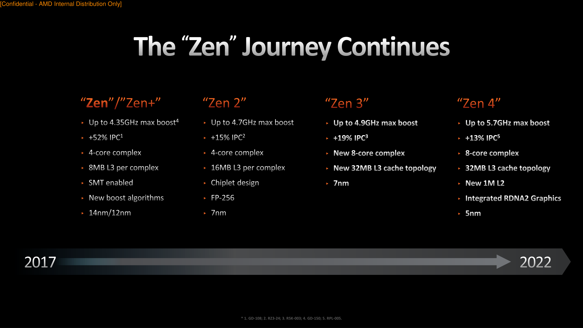
Instead, Zen 4 is a further refinement of AMD’s Zen 3 architecture, with AMD taking advantage of things like the new AM5 platform and TSMC’s 5nm process to further boost performance. There are some important changes here that are allowing AMD to deliver an average IPC increase of 13%, and combined with improvements to enable higher clockspeeds and greater power efficiency for both single-threaded and multi-threaded workloads, no part of AMD’s CPU performance has gone untouched.
Zen 4 Power: More Efficient, More Power-Hungry
We’ll start with a look at power efficiency, since power consumption plays a huge part in the Zen 4 story at both ends of the curve.
By tapping TSMC’s current-generation 5nm, process, AMD is enjoying the advantage of a full node shrink for their CPU cores. Thus far TSMC 5nm (and its 4nm derivative) is proving to be the powerhouse process of its generation, as TSMC’s clients have seen some solid gains in power efficiency and transistor density moving from 7nm to 5nm. Meanwhile TSMC’s competitors are either struggling by delivering less efficient 4nm-class nodes (Samsung), or they’ve yet to deliver a 4nm-class node at all (Intel). In other words, for the moment TSMC’s 5nm-class nodes are as good as it gets, putting AMD in a great position to take advantage of the benefits.
Coupled with this are all of the various platform power improvements that come with AM5 and the new 6nm IOD. These include the 3 variable power rails, SVI3 VRM monitoring, and AMD’s lower-power Infinity Fabric Links. As a result, the Ryzen 7000 chips enjoy a significant power efficiency advantage versus the Ryzen 5000 chips.
How much of an improvement, in turn, depends on where on the voltage/frequency curve you end up. As we alluded to earlier when talking about AM5, one of AMD’s design goals was to provide more power to Ryzen 7000 chips so that they could go farther into the vf curve and keep their cores running at a higher frequency in MT-heavy workloads.
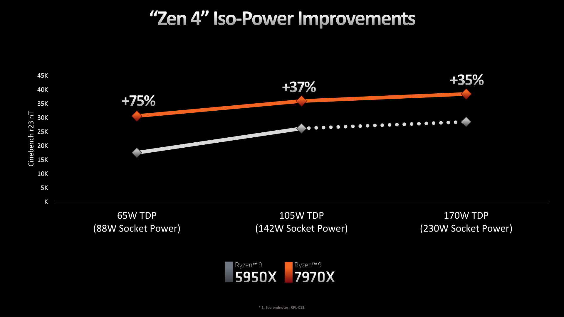
The net result is that, according to AMD’s data, the company is seeing extensive power efficiency gains at lower TDPs. In this case, pitting a 5950X against a 7950X with a maximum socket power of 88 Watts, AMD is seeing a 75% increase in performance on Cinebench R23 nT. This is something of a worst-case scenario for the older Ryzen chip, as it tended to be TDP limited even at is native TDP, and the relatively high idle power draw of the IOD and the rest of the platform further ate into that. As a result, the 5950X needs to pull back on clockspeeds significantly at lower TDPs. For Ryzen 7000/Zen 4 on the other hand, AMD’s newer architecture fairs much better; it still takes a hit from the TDP drop, but not by nearly as much.
Meanwhile, increasing the socket power to 142 (5950X’s stock power) and then to 230W (7950X’s stock power) still produces a significant speed up in performance, but we’re certainly into the area of diminishing returns. In this case the 7950X has a 37% lead and 35% lead at 142W and 230W respectively.
We’ll take a look at more power data for the new Ryzen 7000 chips a bit later in our review, but the basic pattern is clear: Zen 4 can be a very power efficient architecture. But AMD is also discarding some of that efficiency advantage in the name of improving raw performance. Especially in multi-threaded workloads, for high-end chips like the 7950X the performance gains we’re seeing are as much from higher TDPs as they are higher IPCs and improved power efficiency.
This will make AMD’s eventual Zen 4 mobile products (Phoenix Point) an especially interesting product to keep an eye on. The greater focus on power efficiency (and harder cap on top TDPs) means that we may not yet have seen Zen 4 put its best foot forward when it comes to power efficiency.
Clockspeeds: Going Faster Means Being Faster
One way that’s always a good method to improve your CPU performance is just to flat-out increase clockspeeds. Tried and true, this drove the x86 CPU industry for most of its first 30 years before the laws of physics (and specifically, the death of Dennard Scaling) put the brakes on massive generation-on-generation clockspeed gains. Still, AMD and Intel like to squeeze out higher frequencies when they can, and in the case of AMD’s CPU architecture, TSMC’s 5nm process has provided for some nice gains here, finally pushing AMD well over the (stubborn) 5GHz mark.
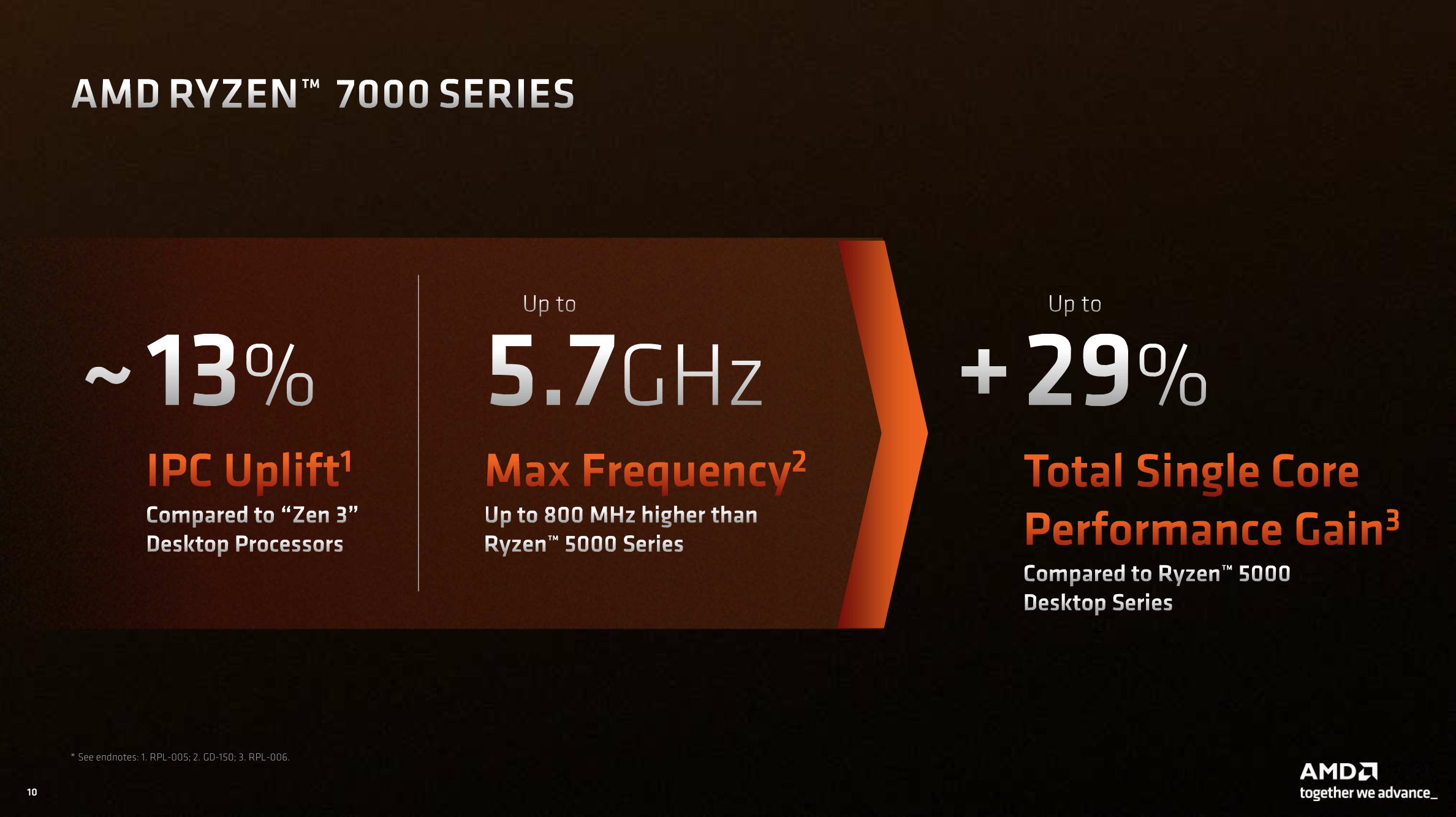
For AMD’s high-end Ryzen 7000 desktop processors, the top turbo frequencies are now as high as 5.7GHz for the Ryzen 9 7950X, and even the slowest Ryzen 5 7600X is rated to hit 5.3GHz. And in both cases, there is still a bit more headroom still when using Precision Boost Optimization 2 (PBO2), allowing chips to potentially eek out another 100MHz or so. For AMD’s top-end part then, we’re looking at a 16% increase in turbo clockspeeds, while the 7600X is clocked some 15% faster than its predecessor.
According to AMD’s engineers, there is no singular magic trick here that has allowed them to boost clockspeeds to the high 5GHz range on Zen 4, nor has the company sacrificed any IPC to allow for higher clockspeeds (e.g. lengthening pipelines). TSMC’s 5nm process sure helped a lot in this regard, but AMD’s technical relationship with TSMC also improved as the company’s CPU engineers became familiar with designing and optimizing CPUs for TSMC’s 7nm and 6nm process nodes. As a result, the two companies were able to better work together to reliably get higher frequencies out of AMD’s CPU cores, with AMD going as far as to integrating some TSMC IP instead of relying on more traditional design partners.
Even with that, Zen 4 actually came in a bit below AMD’s expectations, if you can believe that. According to the company’s engineers, they were hoping to hit 6GHz on this part, something that didn’t quite come to fruition. So AMD’s users will have to settle for just 5.7GHz, instead.
Zen 4 IPC: Getting 13% More
On the other side of the performance equation we have IPC improvements. AMD’s broader focus on platform design for the Ryzen 7000 generation means that the IPC gains aren’t quite as great as what we saw on Zen 3 or Zen 2, but they’re not to be ignored, either. Even without a massive overhaul of AMD’s execution back-end – and with only a moderate update to the front-end – AMD was still able to squeeze out an average IPC gain of 13% across a couple of dozen benchmarks, only 2 percentage points lower than the 15% gains AMD delivered with the Zen 2 architecture in 2019.
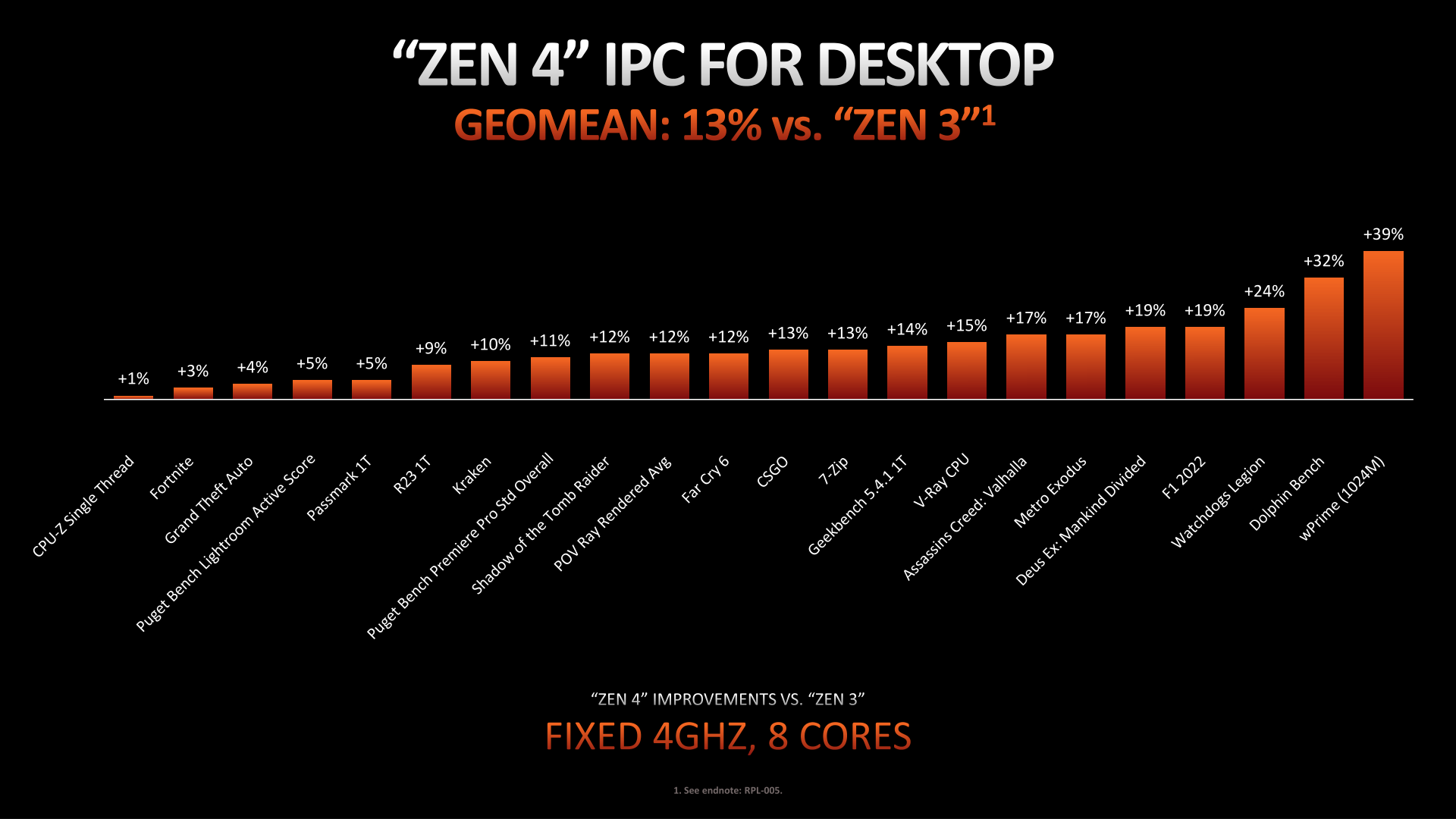
We won’t fixate on any one workload here, but it does run the gamut. At an iso-frequency of 4GHz, Zen 4 delivers anything from a tiny increase to 39% at the top end. In traditional PC performance fashion, the gains from one generation to the next are workload-dependent. So a 13% average does leave plenty of wiggle-room for either greater or lesser gains, as we’ll see in our full benchmark results.
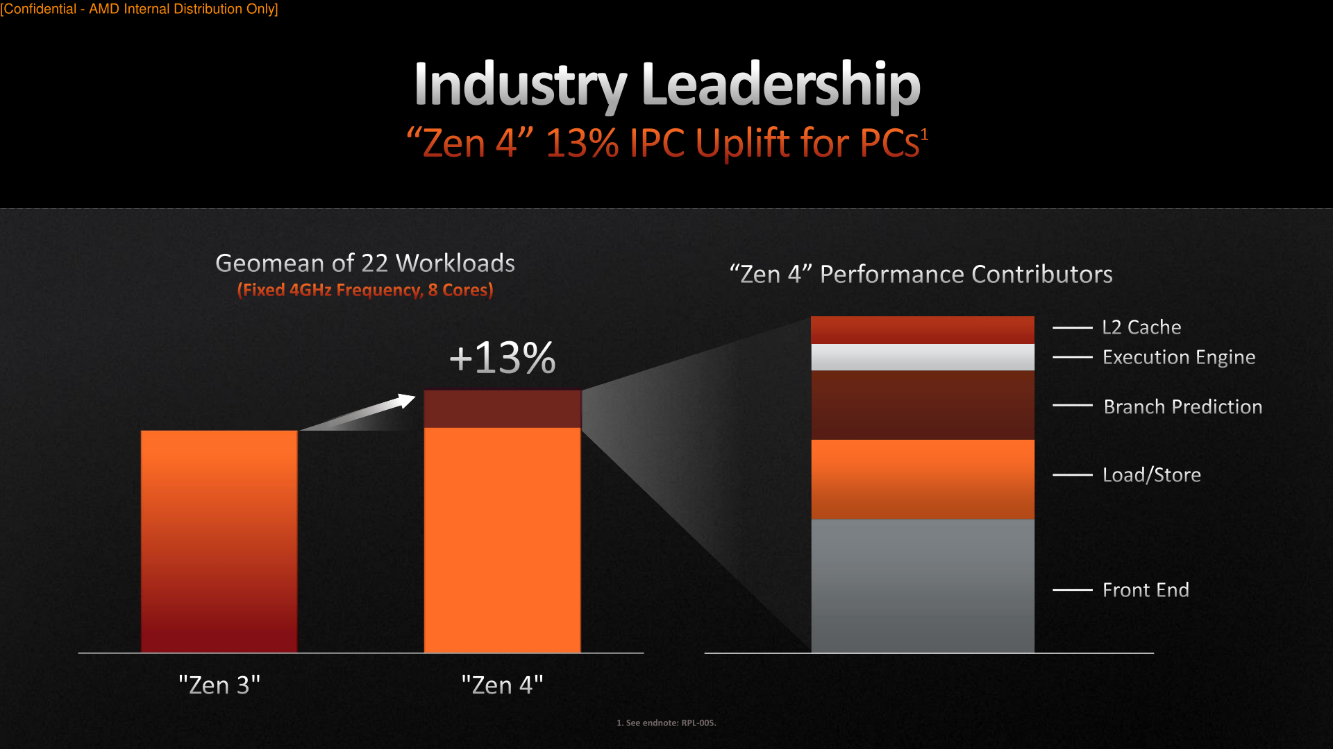
AMD has also provided a handy IPC contributor breakdown, showing where those 13% average gains come from. The single biggest contributor here was Zen 4’s front-end changes, followed by load/store improvements, and then branch prediction improvements.
New Instructions: AVX-512, Automatic IBRS
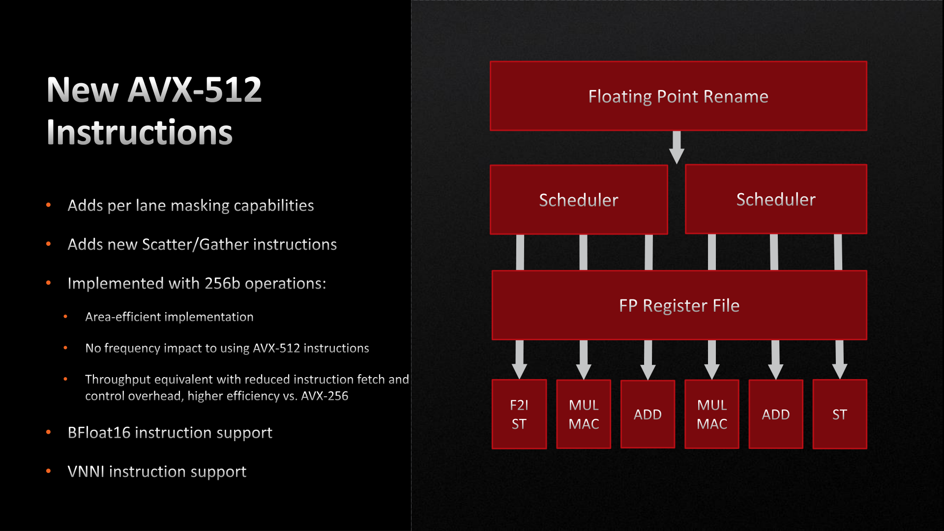
Although Zen 4 is a more modest update to AMD’s CPU architecture, the company still managed to work in a fairly significant update to their instruction set support, with the addition of AVX-512 support.
The latest iteration of the Intel-developed Advanced Vector Extensions (AVX), AVX-512 is a fairly major addition to the AVX suite. Besides increasing the native vector width to 512-bits, AVX also improves the AVX instruction set with a number of new features and data types – a collection of features that keeps growing as Intel continues to add further extensions to AVX-512 itself.
Of particular interest for client CPUs and workloads, AVX-512 adds per-lane masking capabilities – allowing for individual lanes to be masked off rather than breaking up a vector for multiple passes – as well as new data manipulation instructions. This includes additional scatter/gather instructions, and instructions that are useful for neural network processing, such as bfloat16 support and a whole instruction sub-set (VNNI) for deep learning.
AVX-512 has an interesting history that, while we won’t cover in complete details, has left a patchwork of support across the client CPU landscape. While Intel added support in its client CPUs starting with Ice Lake and Rocket Lake (11th Gen Core), Intel also removed support for AVX-512 from their client CPUs starting with Alder Lake (13th Gen Core), owing to the fact that Alder Lake’s mixed-core strategy required that the only instructions used were supported by both the P-cores and E-cores. Which, in the case of the Atom-based Gracemont E-cores, was not available, leading to Intel disabling AVX-512 on Alder Lake parts even though the P-cores did support the new instructions.
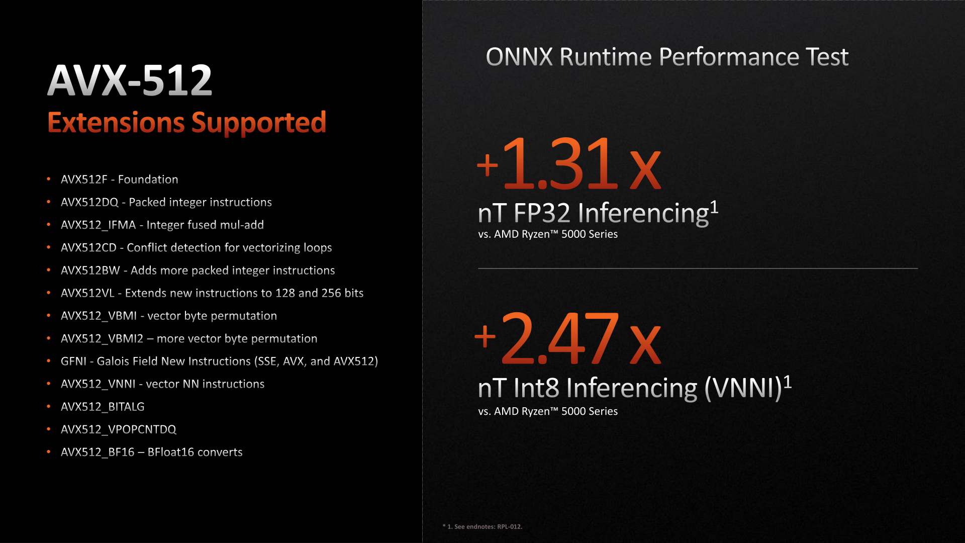
As a result, the introduction of AVX-512 support actually gives AMD an edge over Intel right now. While AMD’s new CPUs can use the newer instruction set, Intel’s cannot, with Alder Lake limited to AVX2 and below.
But the situation is not a slam-dunk for AMD, either. In order to avoid the significant die space and power costs of actually implementing and operating a 512-bit wide SIMD, AMD has made the interesting decision to implement AVX-512 on top of a 256-bit SIMD, which happens to be the same width as Zen 3’s AVX2 SIMD. This means that while AMD can execute AVX-512 instructions, they have to do so over 2 cycles of their 256-bit SIMD. Which means that, on paper, AMD’s vector throughput per cycle per core has not improved from one generation to the next.
None the less, it’s a situation that benefits AMD for a couple of reasons. The first is the performance unlocked by the AVX-512 instructions. AVX-512 instructions are denser (there’s less fetching and control overhead), and some of these additions are instructions that manipulate data in ways that would take several cycles (or more) if implemented using AVX2 instructions. So AMD is still getting performance gains by supporting AVX-512, even without the doubled vector width.
The second benefit is that by keeping their SIMD narrower, AMD isn’t lighting up a billion dense, power-hungry transistors all at once. This is an ongoing challenge for 512-bit native SIMD designs that in Intel’s chips required them to back off on their clockspeeds to stay within their power budgets. So while a wider SIMD would technically be more efficient on pure AVX-512 throughput, the narrower SIMD allows AMD to keep their clockspeeds higher, something that’s particularly useful in mixed workloads where the bottleneck shifts between vector throughput and more traditional serial instructions.
Ultimately, for client CPUs, this is a nice feature to have, but it admittedly wasn’t a huge, market-shifting feature advantage with Rocket Lake. And it’s unlikely to be that way for AMD, either. Instead, the biggest utility for AVX-512 is going to be in the server space, where AMD’s Genoa processors will be going up against Intel Ice Lake (and eventually, Sapphire Rapids) parts with full AVX-512 implementations.
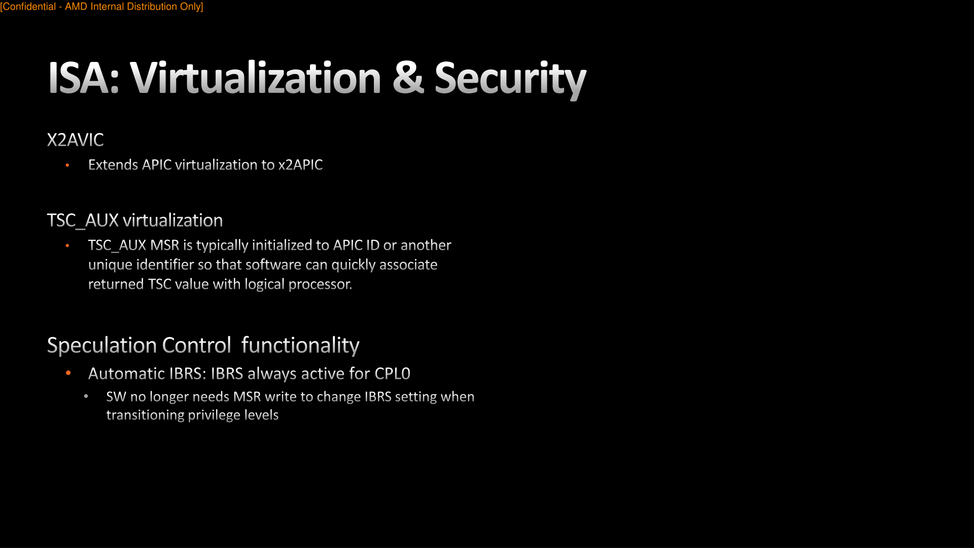
Finally, AMD is also adding/changing a handful of instructions related to security and virtualization. I won’t parrot AMD’s own slide on the matter, but for general desktop users, the most notable of these changes is how AMD is handling speculation control to prevent side-channel attacks. The Indirect Branch Restricted Speculation (IBRS) instruction, which is used on critical code paths to restrict the speculation of indirect branches, is now automatic. Any time a CPU core goes to CPL0/Ring 0 – the kernel ring and thus the most privileged ring – IBRS is automatically turned on, and similarly turned off when the CPU core exits CPL0.
Previously, software would need to specifically invoke IRBS using a model specific register, which although not a deal-breaker, was one more thing for an application (and application programmers) to keep track of in an already complex security landscape. Thus this change doesn’t directly add any new security features, but it makes it much easier to take advantage of an existing one.
Finally, let’s take a look at the Zen 4 microarchitecture’s execution flow in-depth. As we noted before, AMD is seeing a 13% IPC improvement over Zen 3. So how did they do it?
Throughout the Zen 4 architecture, there is not any single radical change. Zen 4 does make a few notable changes, but the basics of the instruction flow are unchanged, especially on the back-end execution pipelines. Rather, many (if not most) of the IPC improvements in Zen 4 come from improving cache and buffer sizes in some respect.
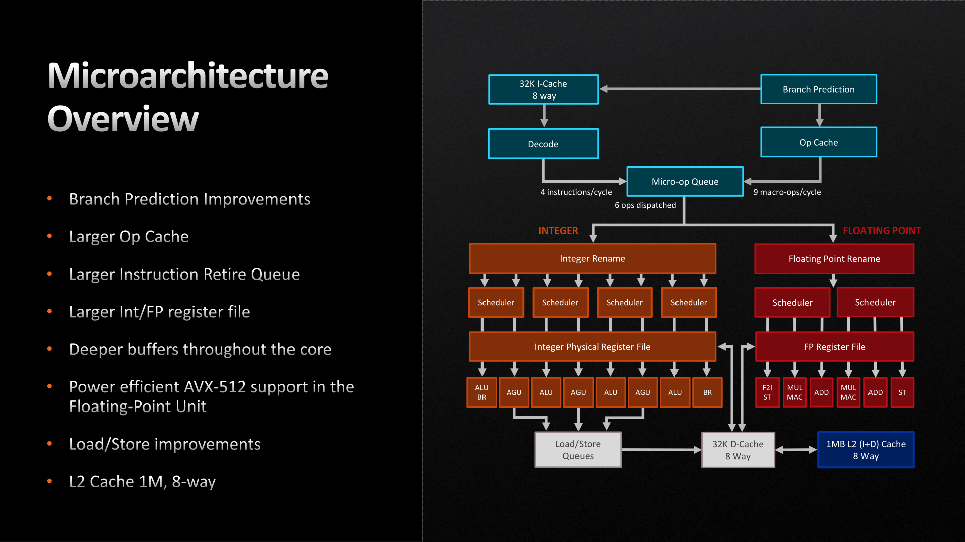
Starting with the front end, AMD has made a few important improvements here. The branch predictor, a common target for improvements given the payoffs of correct predictions, has been further iterated upon for Zen 4. While still predicting 2 branches per cycle (the same as Zen 3), AMD has increased the L1 Branch Target Buffer (BTB) cache size by 50%, to 2 x 1.5k entries. And similarly, the L2 BTB has been increased to 2 x 7k entries (though this is just an ~8% capacity increase). The net result being that the branch predictor’s accuracy is improved by being able to look over a longer history of branch targets.
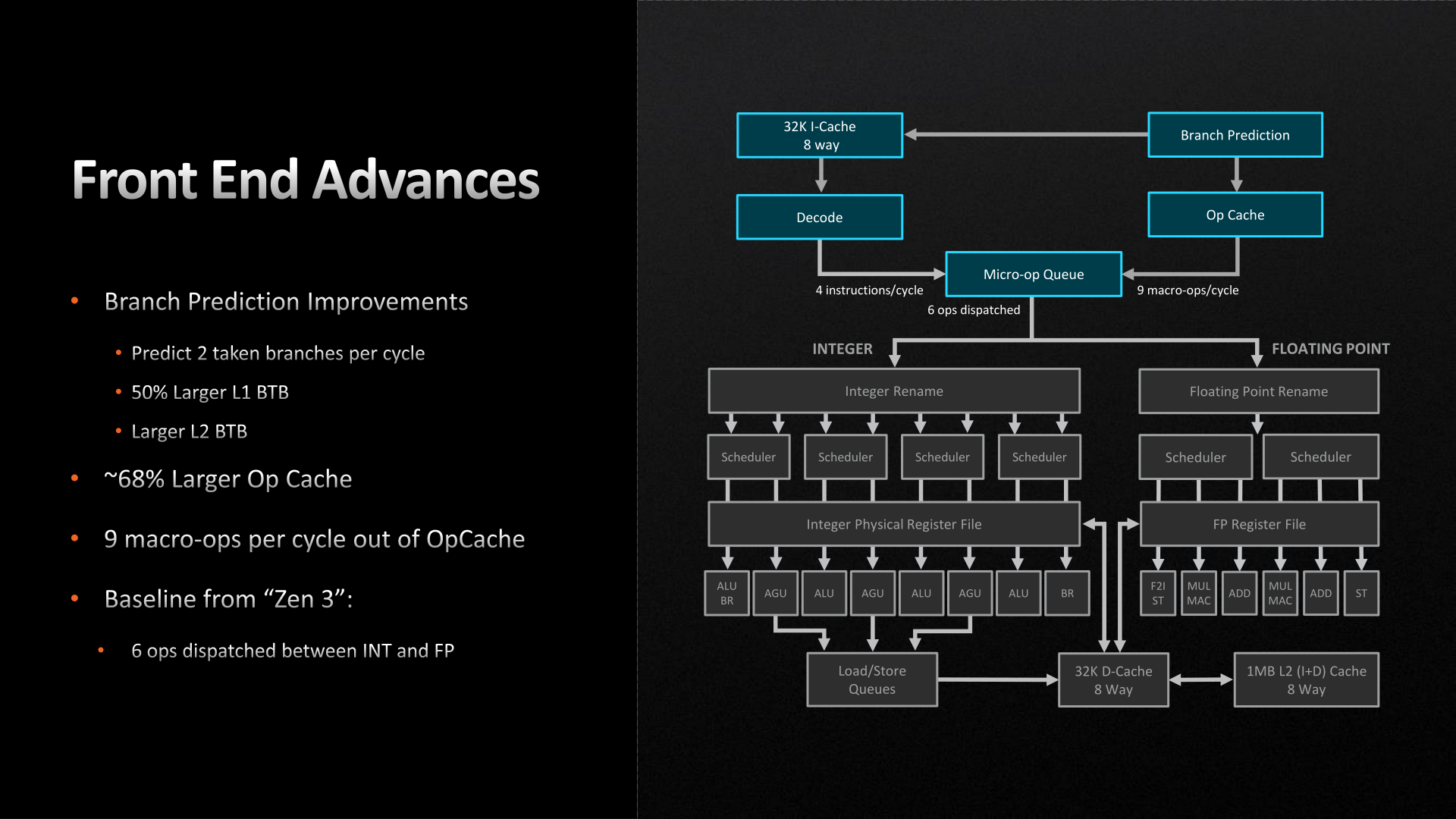
Meanwhile the branch predictor’s op cache has been more significantly improved. The op cache is not only 68% larger than before (now storing 6.75k ops), but it can now spit out up to 9 macro-ops per cycle, up from 6 on Zen 3. So in scenarios where the branch predictor is doing especially well at its job and the micro-op queue can consume additional instructions, it’s possible to get up to 50% more ops out of the op cache. Besides the performance improvement, this has a positive benefit to power efficiency since tapping cached ops requires a lot less power than decoding new ones.
With that said, the output of the micro-op queue itself has not changed. The final stage of the front-end can still only spit out 6 micro-ops per clock, so the improved op cache transfer rate is only particularly useful in scenarios where the micro-op queue would otherwise be running low on ops to dispatch.
Switching to the back-end of the Zen 4 execution pipeline, things are once again relatively unchanged. There are no pipeline or port changes to speak of; Zen 4 still can (only) schedule up to 10 Integer and 6 Floating Point operations per clock. Similarly, the fundamental floating point op latency rates remain unchanged as 3 cycles for FADD and FMUL, and 4 cycles for FMA.
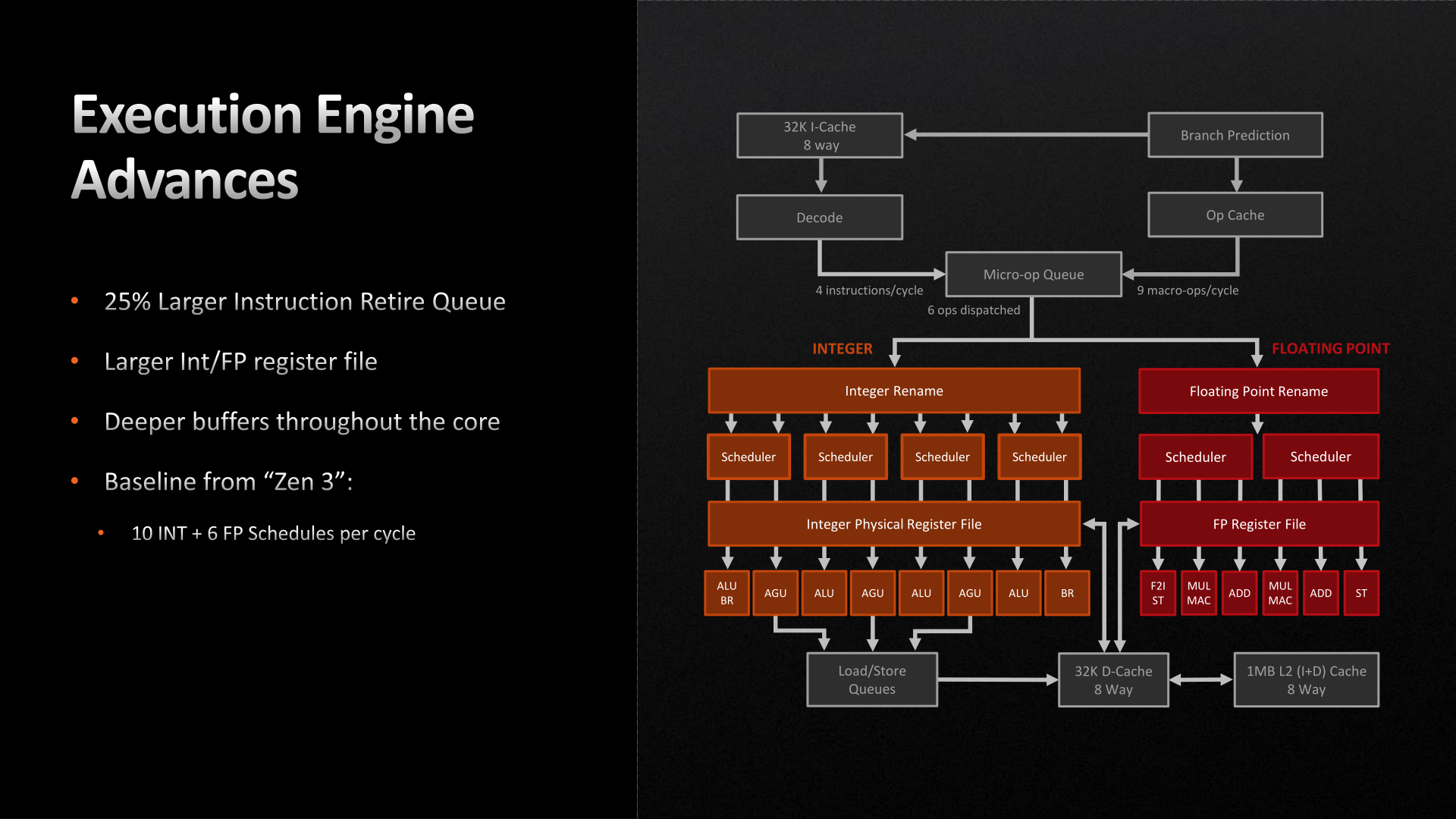
Instead, AMD’s improvements to the back-end of Zen 4 have here too focused on larger caches and buffers. Of note, the retire queue/reorder buffer is 25% larger, and is now 320 instructions deep, giving the CPU a wider window of instructions to look through to extract performance via out-of-order execution. Similarly, the Integer and FP register files have been increased in size by about 20% each, to 224 registers and 192 registers respectively, in order to accommodate the larger number of instructions that are now in flight.
The only other notable change here is AVX-512 support, which we touched upon earlier. AVX execution takes place in AMD’s floating point ports, and as such, those have been beefed up to support the new instructions.
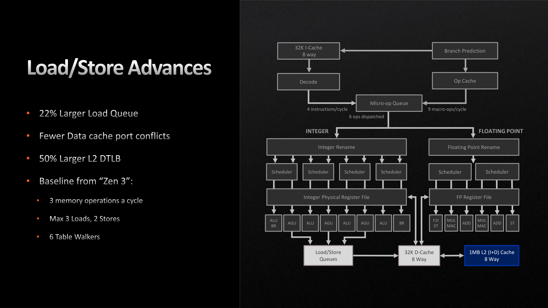
Moving on, the load/store units within each CPU core have also been given a buffer enlargement. The load queue is 22% deeper, now storing 88 loads. And according to AMD, they’ve made some unspecified changes to reduce port conflicts with their L1 data cache. Otherwise the load/store throughput remains unchanged at 3 loads and 2 stores per cycle.
Finally, let’s talk about AMD’s L2 cache. As previously disclosed by the company, the Zen 4 architecture is doubling the size of the L2 cache on each CPU core, taking it from 512KB to a full 1MB. As with AMD’s lower-level buffer improvements, the larger L2 cache is designed to further improve performance/IPC by keeping more relevant data closer to the CPU cores, as opposed to ending up in the L3 cache, or worse, main memory. Beyond that, the L3 cache remains unchanged at 32MB for an 8 core CCX, functioning as a victim cache for each CPU core’s L2 cache.
All told, we aren’t seeing very many major changes in the Zen 4 execution pipeline, and that’s okay. Increasing cache and buffer sizes is another tried and true way to improve the performance of an architecture by keeping an existing design filled and working more often, and that’s what AMD has opted to do for Zen 4. Especially coming in conjunction with the jump from TSMC 7nm to 5nm and the resulting increase in transistor budget, this is good way to put those additional transistors to good use while AMD works on a more significant overhaul to the Zen architecture for Zen 5.
As per our processor testing policy, we take a premium category motherboard suitable for the socket, and equip the system with a suitable amount of memory running at the manufacturer's maximum supported frequency. This is also typically run at JEDEC subtimings where possible. It is noted that some users are not keen on this policy, stating that sometimes the maximum supported frequency is quite low, or faster memory is available at a similar price, or that the JEDEC speeds can be prohibitive for performance.
While these comments make sense, ultimately very few users apply memory profiles (either XMP or other) as they require interaction with the BIOS, and most users will fall back on JEDEC-supported speeds - this includes home users as well as industry who might want to shave off a cent or two from the cost or stay within the margins set by the manufacturer. Where possible, we will extend out testing to include faster memory modules either at the same time as the review or a later date.
The Current CPU Test Suite
For our AMD Ryzen 9 7950X and Ryzen 5 7600X testing, we are using the following test system:
| AMD Ryzen 7000 Series System (DDR5) | |
| CPU | Ryzen 9 7950X ($699) 16 Cores, 32 Threads 170 W TDP Ryzen 5 7600X ($299) |
| Motherboard | GIGABYTE X670E Aorus Master (BIOS 813b) |
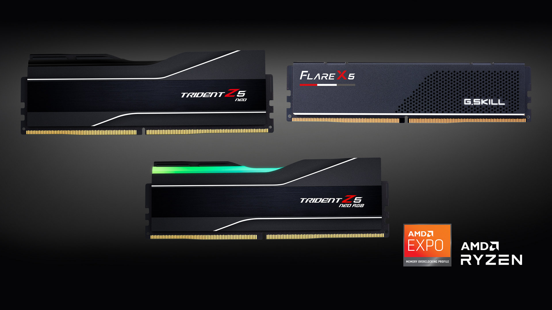
| Memory | G.Skill Trident Z5 Neo 2x16 GB DDR5-5200 CL44 |
| Cooling | EK-AIO Elite 360 D-RGB 360 mm AIO |
| Storage | Crucial MX300 1TB |
| Power Supply | Corsair HX850 |
| GPUs | NVIDIA GeForce RTX 2080 Ti, Driver 496.49 |
| Operating Systems | Windows 11 21H1 |
As we are in a transitional period between our current CPU 2021 suite and data, and optimizing our CPU 2023 suite with different data comparisons required, we have included a varied selection of benchmarks for this review. This ranges from our traditional un-updatable Google Octane 2.0 web test, through a variety of rendering benchmarks such as CineBench R23 and Blender, to encoding, and all the way to our more scientific-related tests.
With our processor reviews, especially on a new generational product such as AMD's Ryzen 9 7950X, we also include SPEC2017 data to account for any increases (or decreases) to generational single-threaded and multi-threaded performance. It should be noted that due to the terms of the SPEC license because our benchmark results are not vetted directly by the SPEC consortium, we have to label them as ‘estimated’. The benchmark is still run and we get results out, but those results have to have the ‘estimated’ label.
Moving Foward to Our CPU 2023 Suite: What to Expect
Looking ahead to our updated CPU 2023 suite, we've updated some of our existing benchmarks to the latest and current versions (as of Sept 22) such as Blender 3.3. In terms of benchmarks from our CPU 2021 suite, we've included benchmarks such as Dwarf Fortress, Factorio, and Dr. Ian Cutress's 3DPMv2 and Crysis CPU benchmarks.
We've also added some completely new benchmarks and workloads to our suite, including an update to Blender (v3.3), C-Ray 1.1 rendering, as well as more scientific-based workloads such as SciMark 2.0 and Primesieve 1.9.0. We have also decided to add UL's latest Procyon suite which measures overall system performance when doing tasks such as office-based tasks, as well as video, and photo editing.
As it stands, we have also updated our pool of games going forward into 2023 and beyond, including the latest F1 2022 racing game, the CPU-intensive Total War Warhammer 3 real-time strategy, and the popular Hitman 3 assassin-based title.
Our aim is to provide varying levels of data points across a variety of different workloads, instruction sets, and tasks. Going forward, we will keep our CPU 2023 suite updated as frequently as possible, and when we have a consistent and suitable number of data points, it will feature on our Bench database as we continue testing new and older CPUs for varying data points.
Some of these new benchmarks will make an appearance in this review, while others won't. Our aim is to assess and subjugate our way through whatever CPUs we have on hand to add vital data points. However, some parts of our CPU 2023 suite are still under testing and it should make a full debut in our next CPU review.
As the core count of modern CPUs is growing, we are reaching a time when the time to access each core from a different core is no longer a constant. Even before the advent of heterogeneous SoC designs, processors built on large rings or meshes can have different latencies to access the nearest core compared to the furthest core. This rings true especially in multi-socket server environments.
But modern CPUs, even desktop and consumer CPUs, can have variable access latency to get to another core. For example, in the first generation Threadripper CPUs, we had four chips on the package, each with 8 threads, and each with a different core-to-core latency depending on if it was on-die or off-die. This gets more complex with products like Lakefield, which has two different communication buses depending on which core is talking to which.
If you are a regular reader of AnandTech’s CPU reviews, you will recognize our Core-to-Core latency test. It’s a great way to show exactly how groups of cores are laid out on the silicon. This is a custom in-house test, and we know there are competing tests out there, but we feel ours is the most accurate to how quick an access between two cores can happen.
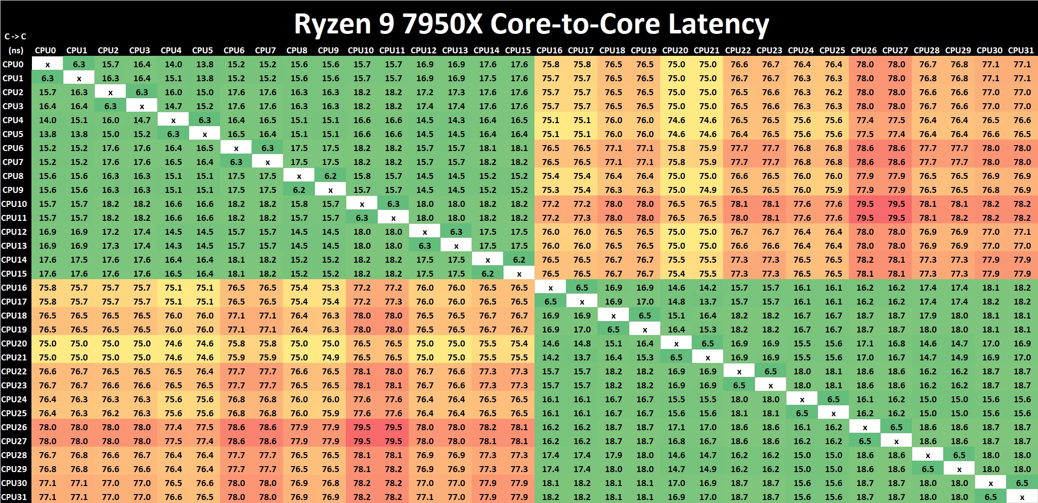
Click to enlarge (lots of cores and threads = lots of core pairings)
Comparing core to core latencies from Zen 4 (7950X) and Zen 3 (5950X), both are using a two CCX 8-core chiplet design, which is a marked improvement over the four CCX 16-core design featured on the Zen 2 microarchitecture, the Ryzen 9 3950X. The inter-core latencies within the L3 cache range from between 15 ns and 19 ns. The inter-core latencies between different cores within different parts of the CCD show a larger latency penalty of up to 79.5 ns, which is something AMD should work on going forward, but it's an overall improvement in cross CCX latencies compared to Zen 3. Any gain is still a gain.
Even though AMD has opted for a newer and more 'efficient' IOD which is based on TSMC's 6 nm node. It is around the same size physically as the previous AMD IOD on Zen 3 manufactured on GlobalFoundries 12 nm node, but with a much larger transistor count. Within the IOD is the newly integrated RDNA 2 graphics, although this isn't typical iGPU in the sense that an APU is. A lot of the room on the IOD is made up of the DDR5 memory controller or IMC, as well as the chips PCIe 5.0 lanes, and of course, connects to the logic through its primary interconnect named Infinity Fabric. All of these variables play a part on power, latency, and operation.
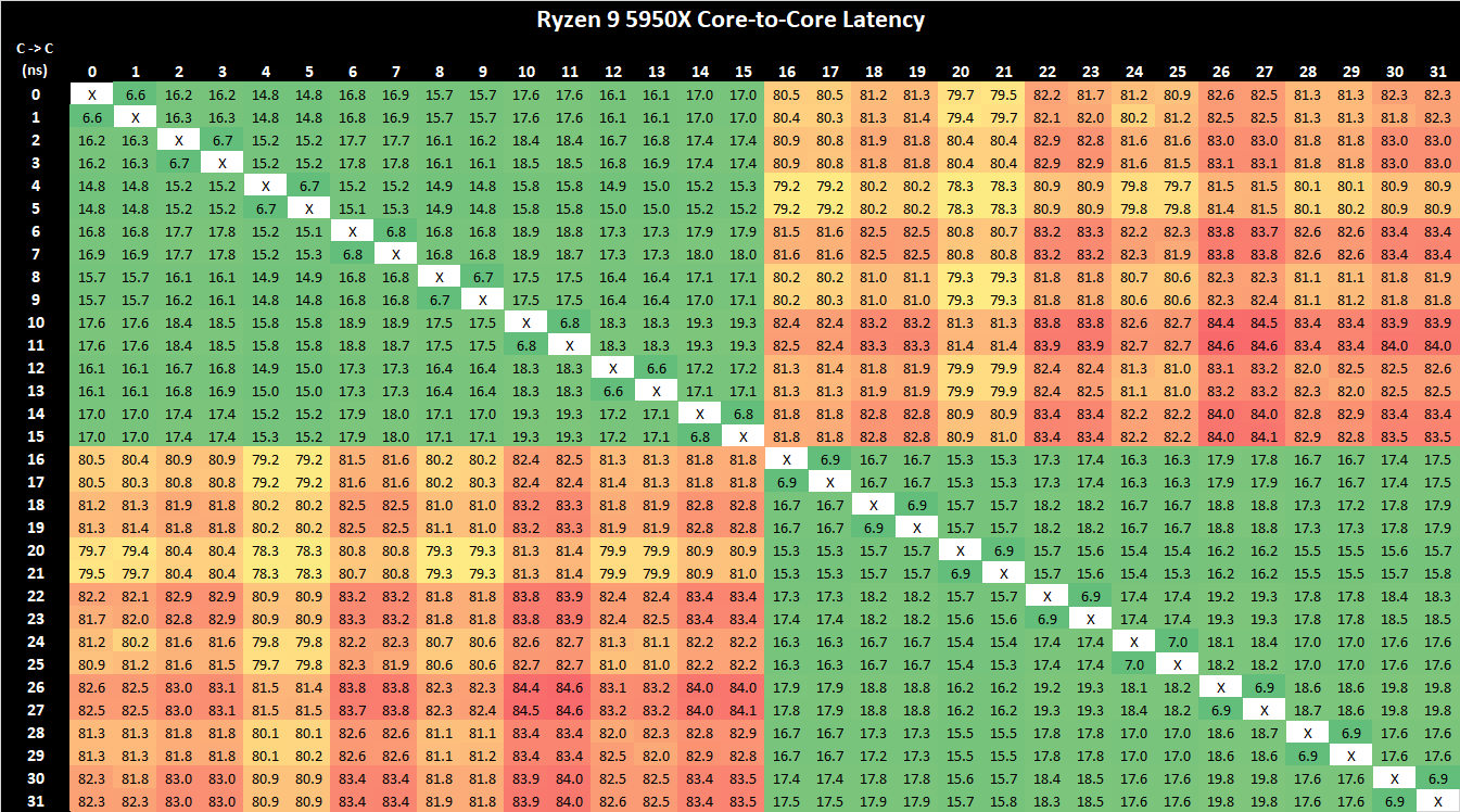
AMD Ryzen 9 5950X Core-to-Core Latency results
It's actually astounding how similar the latency performance of the Ryzen 9 7950X (Zen 4) is when compared directly to the Ryzen 9 5950X (Zen 3), despite being on the new 5 nm TSMC manufacturing process. Even with a change of IOD, but with the same interconnect, the inter-core latencies within the Ryzen 9 7950X are great in terms of cores within the same core complex; latency does degrade when pairing up with a core in another chiplet, but this works and AMD's Ryzen 5000 series proved that the overall penalty performance is negatable.
SPEC2017 is a series of standardized tests used to probe the overall performance between different systems, different architectures, different microarchitectures, and setups. The code has to be compiled, and then the results can be submitted to an online database for comparison. It covers a range of integer and floating point workloads, and can be very optimized for each CPU, so it is important to check how the benchmarks are being compiled and run.
We run the tests in a harness built through Windows Subsystem for Linux, developed by Andrei Frumusanu. WSL has some odd quirks, with one test not running due to a WSL fixed stack size, but for like-for-like testing it is good enough. Because our scores aren’t official submissions, as per SPEC guidelines we have to declare them as internal estimates on our part.
For compilers, we use LLVM both for C/C++ and Fortan tests, and for Fortran we’re using the Flang compiler. The rationale of using LLVM over GCC is better cross-platform comparisons to platforms that have only have LLVM support and future articles where we’ll investigate this aspect more. We’re not considering closed-sourced compilers such as MSVC or ICC.
clang version 10.0.0

clang version 7.0.1 (ssh://git@github.com/flang-compiler/flang-driver.git

 24bd54da5c41af04838bbe7b68f830840d47fc03)
-Ofast -fomit-frame-pointer

-march=x86-64

-mtune=core-avx2

-mfma -mavx -mavx2
Our compiler flags are straightforward, with basic –Ofast and relevant ISA switches to allow for AVX2 instructions.
To note, the requirements for the SPEC licence state that any benchmark results from SPEC have to be labelled ‘estimated’ until they are verified on the SPEC website as a meaningful representation of the expected performance. This is most often done by the big companies and OEMs to showcase performance to customers, however is quite over the top for what we do as reviewers.
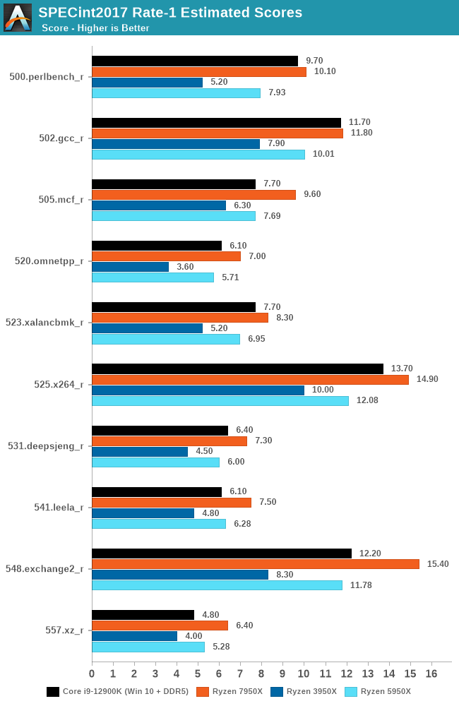
Starting off with single-threaded performance in SPECint2017, we can see that AMD's new Zen 4 core performs when compared directly with its previous Zen 3 and even more so, its Zen 2 microarchitecture. In 500.perlbench_r, the Ryzen 9 7950X has a 27% uplift over the previous Zen 3 based Ryzen 9 5950X, with a massive 94% uplift in single-threaded performance over the Zen 2 based Ryzen 9 3950X. This in itself is impressive, with similar levels of performance increase in other SPECint2017 tests such as a 23% increase over the previous generation in 525.x264_r and 30% in the 548.exchange2_r test.
The performance increase can be explained by a number of variables, including the switch from DDR4 to DDR5 memory, a large increase in clock speed, as well as the inclusion of the AVX-512 instruction set, albeit using two 256-bit pumps. AMD claims to have done this to avoid large changes to the frequencies under load, but the use cases for AVX-512 is much more limited than most instruction sets.
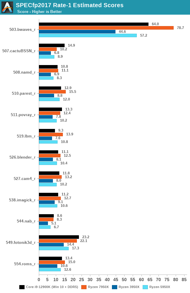
Moving onto our SPECfp2017 1T results, we see a similar increase in performance as in the previous set of 1T-tests. Focusing on the 503.bwaves_r, we are seeing an uplift of 37% over Zen 3. Interestingly, the performance in 549.fotonik3d, we see an increase of around 27% over the Ryzen 9 3950X, although Intel's Alder Lake architecture which is also on DDR5 is outperforming the Ryzen 9 7950X.
Perhaps the biggest increase in Zen 4's improvement in IPC over Zen 3 is through doubling the L2 cache on the 7950X (16MB) versus the 5950X (8MB). Similarly, both the Ryzen 9 7950X and 5950X have a large pool of L3 cache (64MB), but the 7950X boosts up to 5.7 GHz on a single core providing the core temperature is below 50°C, or 5.6 GHz if above 50°C.
As it stands at the time of writing, AMD's Ryzen 9 7950X is the clear leader in single-core IPC performance, with a pretty comprehensive increase in IPC performance over Zen 3. Although Intel's Alder Lake (12th Gen) provided gains over AMD's Ryzen 5000 series in a multitude of ways including frequency, optimizations, and its complex hybrid architecture. There is no doubt that the latest Zen 4 microarchitecture using TSMC's 5 nm node gives AMD the single-thread performance crown, and in terms of single-threaded applications, it's the most powerful x86 desktop processor right now.
Although single-threaded performance is important and Zen 4 has a clear advantage here, multi-threaded performance is also very important. Some variables to consider when evaluating multi-threaded performance is that desktop processor designs typically boost a single core higher, with the rest lagging in frequency behind to either stay under the thermal (TJMax) or power (TDP) envelopes. Some manufacturing processes are more efficient by design due to extensive R+D and product management, with Zen 4 looking to be much more in terms of perf per watt over Intel's Alder Lake architecture.
In the instance of the AMD Ryzen 9 7950X, it has a clear advantage over its predecessors in that it not only has a higher single core boost (5.7 GHz versus 4.9 GHz), but it also has a higher TDP than the Ryzen 9 5950X (170 W versus 105 W. This increase in TDP not only allows for a higher frequency, but it allows for a higher frequency spread across all of the cores when under full load.
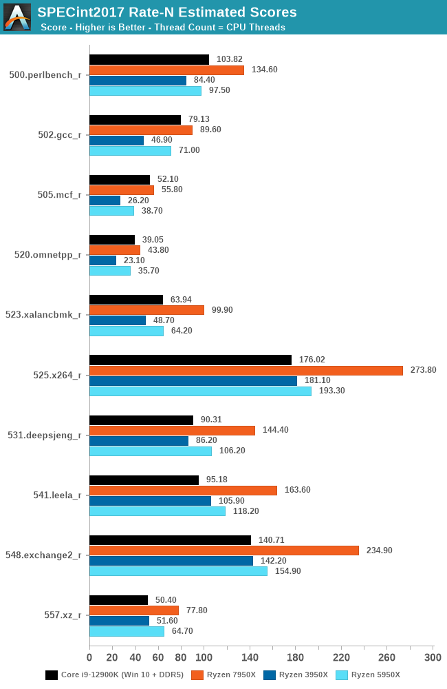
Opening up our look at our SPECint2017 NT results, and we see a similar uplift in performance gains as we did in the single-threaded tests. In tests such as 500.perlbench_r, the Ryzen 9 7950 is 38% ahead of AMD's previous generation Ryzen 9 5950X, which is impressive. In 523_.xalanbmk_r, the Ryzen 9 7950 is 55% ahead of the Ryzen 9 5950X, and over 100% better in performance over the Zen 2-based Ryzen 9 3950X.
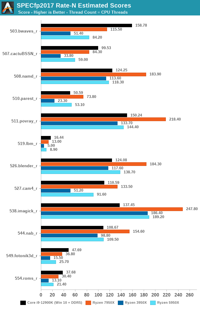
In our SPECfp2017 NT testing, certain workloads such as in 538.imagick_r showed massive increases in performance over previous generations, with a 30% uplift in performance over Zen 3. The difference here between Zen 3 and Zen 2 was marginal (10%), but Zen 4 is a more efficient core architectural design, with many improvements across the board playing a hand here; the switch to DDR5 versus DDR4, more cache per core, higher frequency, higher TDP, etc.
Overall AMD's Zen 4 architectural differences and improvements show that not only does AMD have the crown for single-threaded performance, but it's also ahead in multi-threaded performance too, at least from our SPEC2017 testing. As always when Intel or AMD makes a claim on IPC performance increases, AMD seems to be about right with claims of around 29% in ST performance and even more so in MT performance.
Our previous set of ‘office’ benchmarks has often been a mix of science and synthetics, so this time we wanted to keep our office section purely on real-world performance. We've also incorporated our power and science testing into this section too.
In this version of our test suite, all the science-focused tests that aren’t ‘simulation’ work are now in our science section. Where possible these benchmarks have been optimized with the latest in vector instructions.
We are using DDR5 memory on the Ryzen 9 7950X and Ryzen 5 7600X, as well as Intel's 12th Gen (Alder Lake) processors at the following settings:
- DDR5-5200 CL44 - Ryzen 7000
- DDR5-4800 (B) CL40 - Intel 12th Gen
All other CPUs such as Ryzen 5000 and 3000 were tested at the relevant JEDEC settings as per the processor's individual memory support with DDR4.
Power
The nature of reporting processor power consumption has become, in part, a dystopian nightmare. Historically the peak power consumption of a processor, as purchased, is given by its Thermal Design Power (TDP, or PL1). For many markets, such as embedded processors, that value of TDP still signifies the peak power consumption. For the processors we test at AnandTech, either desktop, notebook, or enterprise, this is not always the case.
Modern high-performance processors implement a feature called Turbo. This allows, usually for a limited time, a processor to go beyond its rated frequency. Exactly how far the processor goes depends on a few factors, such as the Turbo Power Limit (PL2), whether the peak frequency is hard coded, the thermals, and the power delivery. Turbo can sometimes be very aggressive, allowing power values 2.5x above the rated TDP.
AMD and Intel have different definitions for TDP but are broadly speaking, applied the same. The difference comes from turbo modes, turbo limits, turbo budgets, and how the processors manage that power balance. These topics are 10000-12000 word articles in their own right, and we’ve got a few articles worth reading on the topic.
- Why Intel Processors Draw More Power Than Expected: TDP and Turbo Explained
- Talking TDP, Turbo and Overclocking: An Interview with Intel Fellow Guy Therien
- Reaching for Turbo: Aligning Perception with AMD’s Frequency Metrics
- Intel’s TDP Shenanigans Hurts Everyone
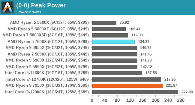
Looking at the results of our Peak Power test, the Ryzen 9 7950X topped out at 221.8 W, which is around 30% higher than the TDP of 170 W it comes with. As stated by AMD, the Power Package Tracking or PPT limit for AM5 motherboards when used with 170W TDP Ryzen 7000 SKUs will be 230 W. Still, while it draws more power than its generational predecessors such as Zen 3 and Zen 2, the Zen 4-based Ryzen 7000 series benefits from higher core clock speeds, a higher single core boost frequency, as well as other implementations around TSMC's 5 nm manufacturing process.
The AMD Ryzen 5 7600X is more aimed at the mid-range, and as such has a lower overall power draw, with the peak power figures in our testing reaching 134.3 W. This is around the same levels of power draw as the Ryzen 9 3950 X, the Ryzen 9 5900X, and the Ryzen 7 5800X. Per AMD's specifications, the Ryzen 5 7600X has a TDP of 105 W, with around a 27 % variance in peak power compared to TDP.
From our testing, so far, it seems that Ryzen 7000 when combined with a premium X670E motherboard allows for up to 30% in terms of extra power allowances for higher single-core boost and overall faster all-core frequencies.
Web
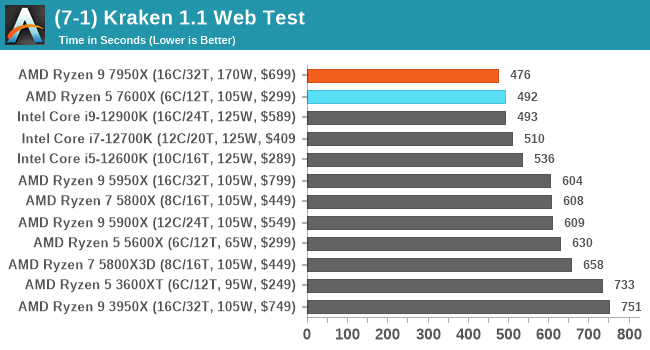
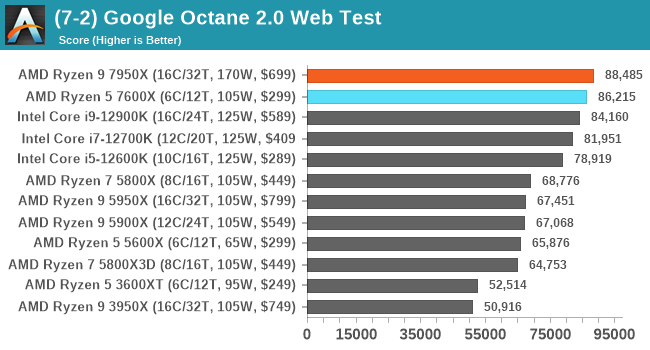
In our web tests, the overall improvements in IPC, frequency, clock speeds, and the switch to DDR5 all play a part in performance here. Both the Ryzen 9 7950X and Ryzen 7 7600X top our charts in regards to web testing, although performance isn't as apparent as it should be in other areas.
Science
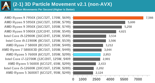
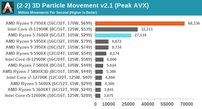
For our 3DPM v2.1 testing, we added in the Intel Core i9-11900K (Rocket Lake) to show performance across AVX workloads. Although Intel officially fused off the AVX2/512 extensions on Alder Lake which did cause a little controversy and gave the impression that AVX-512 on consumer platforms was dead. AMD clearly believes the opposite, as it has implemented it so that AVX-512 runs two cycles over a 256-bit wide instruction. The performance of the Ryzen 9 7950X here is phenomenal, although the Core i9-11900K which did indeed feature AVX instruction sets in the silicon, is still better than the Ryzen 5 7600X with AVX workloads.
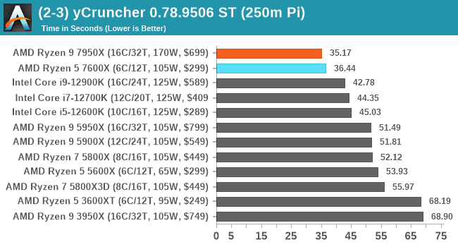
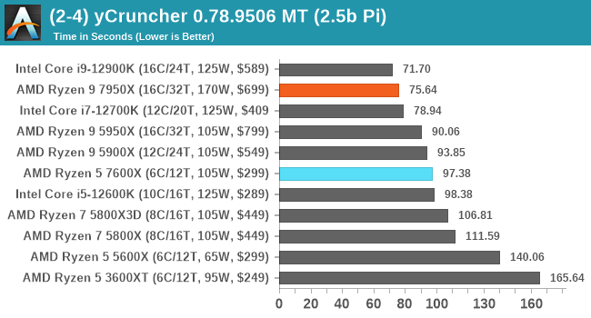
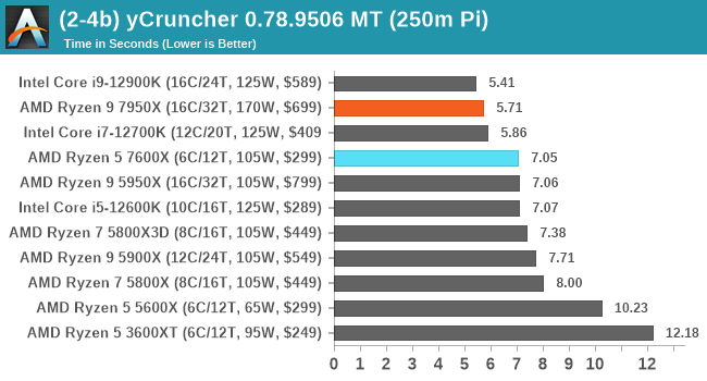
Focusing on our more science-based tests, both the Ryzen 9 7950X and Ryzen 5 7600X perform well against the competition. In our 3DPMv2.1 test in non-AVX, the Ryzen 9 7950X provided a jump of 35% in performance against the previous generation Ryzen 9 5950X processor.
Interestingly, in our yCruncher 0.78 test, the Ryzen 9 7950X and the Core i9-12900K trade blows consistently, although the Ryzen 5 7600X performs well for its price point.
Simulation and Science have a lot of overlap in the benchmarking world, however for this distinction we’re separating into two segments mostly based on the utility of the resulting data. The benchmarks that fall under Science have a distinct use for the data they output – in our Simulation section, these act more like synthetics but at some level are still trying to simulate a given environment.
One of the interesting elements on modern processors is encoding performance. This covers two main areas: encryption/decryption for secure data transfer, and video transcoding from one video format to another.
In the encrypt/decrypt scenario, how data is transferred and by what mechanism is pertinent to on-the-fly encryption of sensitive data - a process by which more modern devices are leaning to for software security.
Video transcoding as a tool to adjust the quality, file size and resolution of a video file has boomed in recent years, such as providing the optimum video for devices before consumption, or for game streamers who are wanting to upload the output from their video camera in real-time. As we move into live 3D video, this task will only get more strenuous, and it turns out that the performance of certain algorithms is a function of the input/output of the content.
We are using DDR5 memory on the Ryzen 9 7950X and Ryzen 5 7600X, as well as Intel's 12th Gen (Alder Lake) processors at the following settings:
- DDR5-5200 CL44 - Ryzen 7000
- DDR5-4800 (B) CL40 - Intel 12th Gen
All other CPUs such as Ryzen 5000 and 3000 were tested at the relevant JEDEC settings as per the processor's individual memory support with DDR4.
Simulation
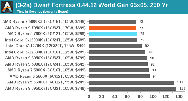
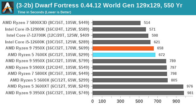
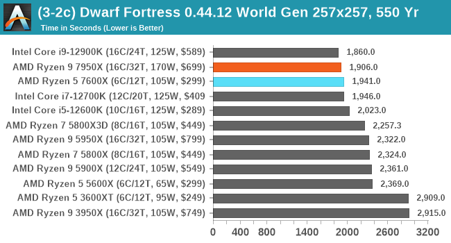
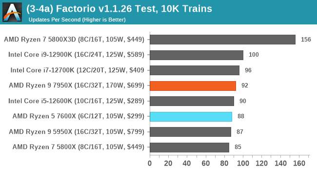
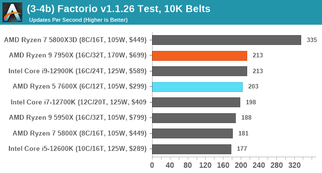
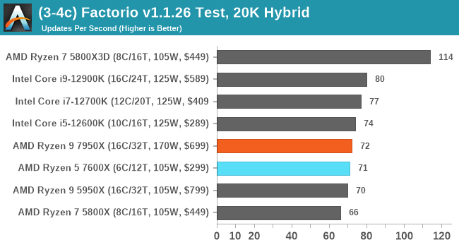
Starting with the Dwarf Fortress section of our simulation suite, the performance of the Ryzen 9 7950X and Ryzen 5 7600X is inconsistent, to say the least. In the smaller of our three Dwart Fortress tests, there's around 2-3% difference between the Ryzen 7000 chips, the Core i9-12900K and Core i7-12700K, and AMD's impressive Ryzen 7 5800X3D with its incredibly large 96 MB pool of cache to play with.
In the larger Dwarf Fortress workloads, and the Alder Lake based Core i9-12900K, the Core i7-12700K and the Core i5-12600K show better scope for performance, with the exception being the Ryzen 7 5800X3D which due to its large 3D V-Cache, keeps the pressure on Intel.
Looking at performance in our Factorio benchmarks, the AMD Ryzen 7 5800X3D with its 3D V-Cache is streets ahead of the competition, with both the Ryzen 9 7950X and Ryzen 5 7600X both lagging behind considerably. Comparing Ryzen 7000 to Intel's Alder Lake, Alder Lake has the overall advantage here, even with the many optimizations and improvements that Zen 4 brings to the table.
Encoding
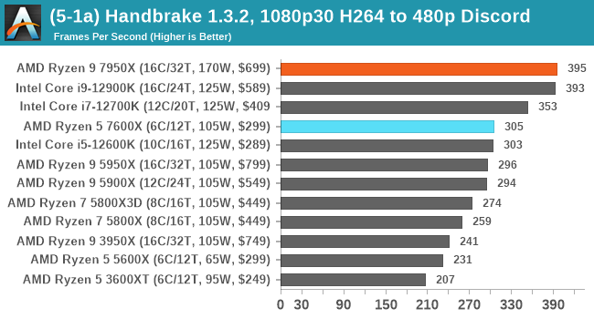
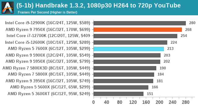
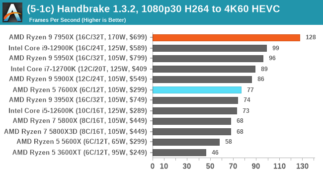
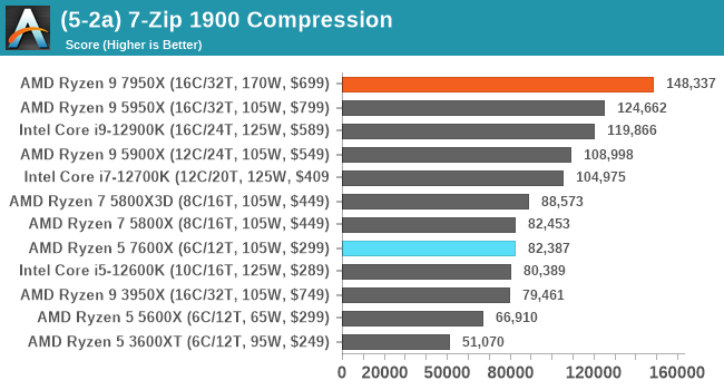
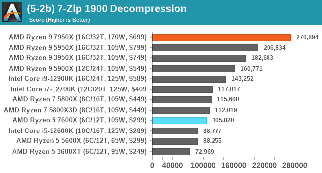
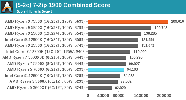
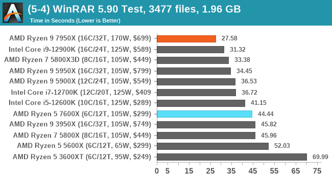
Focusing on encoding, and the Ryzen 9 7950X is the clear winner, beating the Core i9-12900K in all but one of the Handbrake tests (1080p30). The Ryzen 5 7600X trades blows with last generation Ryzen 7 5800X, which is an improvement within itself, as the Ryzen 5 5600X does lag behind the rest of the pack.
Rendering tests, compared to others, are often a little more simple to digest and automate. All the tests put out some sort of score or time, usually in an obtainable way that makes it fairly easy to extract. These tests are some of the most strenuous in our list, due to the highly threaded nature of rendering and ray-tracing, and can draw a lot of power. If a system is not properly configured to deal with the thermal requirements of the processor, the rendering benchmarks is where it would show most easily as the frequency drops over a sustained period of time. Most benchmarks in this case are re-run several times, and the key to this is having an appropriate idle/wait time between benchmarks to allow for temperatures to normalize from the last test.
We are using DDR5 memory on the Ryzen 9 7950X and Ryzen 5 7600X, as well as Intel's 12th Gen (Alder Lake) processors at the following settings:
- DDR5-5200 CL44 - Ryzen 7000
- DDR5-4800 (B) CL40 - Intel 12th Gen
All other CPUs such as Ryzen 5000 and 3000 were tested at the relevant JEDEC settings as per the processor's individual memory support with DDR4.
Rendering
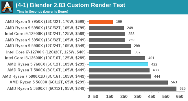
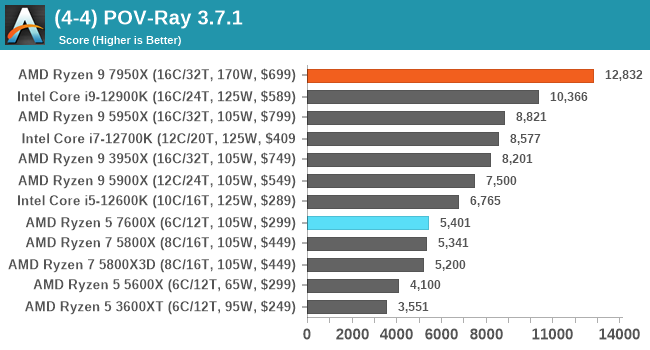
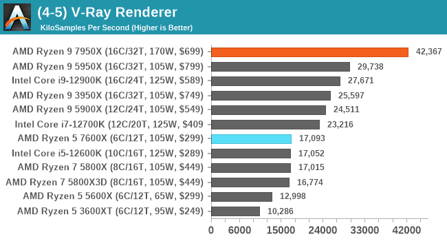
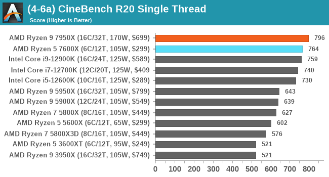
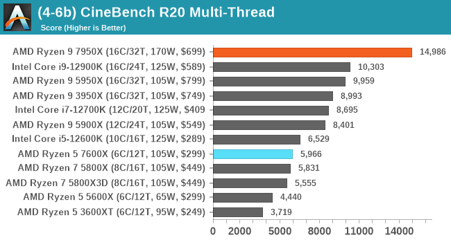
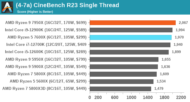
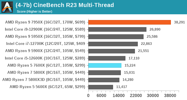
Digesting the results of our rendering focused tests, and yeah, the Ryzen 9 7950X is an animal when it comes to multi-threaded rendering performance. Starting off with CineBench R23 which is one of the most popular benchmarks users rely on for judging performance, the 7950X is ahead by around 24% in the single-threaded test, and an astonishingly large 49 to 50% quicker in the multi-threaded test. For comparison against Intel, it only beats the Core i9-12900K by 3% in the single-threaded section, but it's over 42% more effective in R23 MT performance which is very impressive.
It seems that the more cores and threads that are being used, the more effective AMD's Zen 4 is at stretching its legs over Intel's Alder Lake.
Below is some testing from our upcoming CPU 2023 suite update, including an updated version of Blender (v3.3) with multiple tests, as well as a C-Ray benchmark.
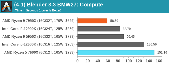

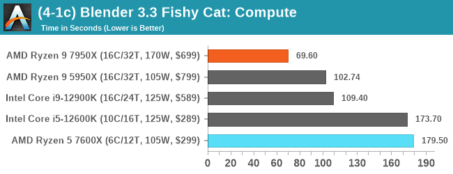
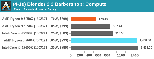
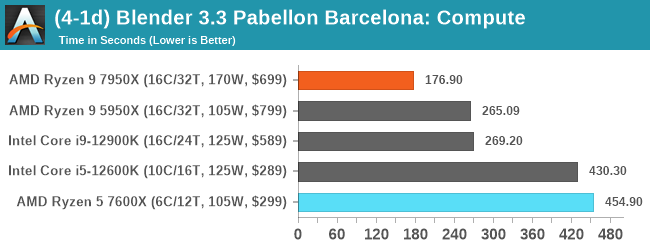
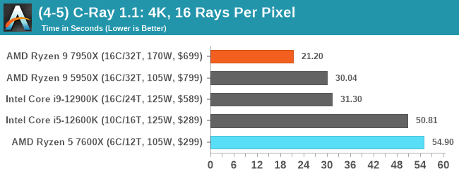
Looking at the results of our new rendering tests, we can see that the AMD Ryzen 9 7950X reigns supreme. Even the previous generation Ryzen 9 5950X (Zen3) performs well here, with sixteen full-sized cores, and not hybrid designed architectures like the Core i9-12900K.
Focusing on the cheaper and more affordable Ryzen 5 7600X, it has similar levels of performance to the Ryzen 7 5800X in rendering; it is worth reminding you that the Ryzen 5 7600X's MSRP is $150 cheaper than what the Ryzen 7 5800X launched for ($299 versus $449). That's a solid gain in value comparing Zen 4 to the previous Zen 3 architectures.
In order to gather data to compare with older benchmarks, we are still keeping a number of tests under our ‘legacy’ section. This includes all the former major versions of CineBench (R15, R11.5, R10) as well as Geekbench 4 and 5. We won’t be transferring the data over from the old testing into Bench, otherwise, it would be populated with 200 CPUs with only one data point, so it will fill up as we test more CPUs like the others.
We are using DDR5 memory on the Ryzen 9 7950X and Ryzen 5 7600X, as well as Intel's 12th Gen (Alder Lake) processors at the following settings:
- DDR5-5200 CL44- Ryzen 7000
- DDR5-4800 (B) CL40 - Intel 12th Gen
All other CPUs such as Ryzen 5000 and 3000 were tested at the relevant JEDEC settings as per the processor's individual memory support with DDR4.
Legacy
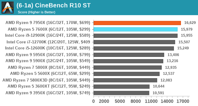
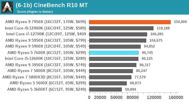
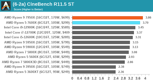
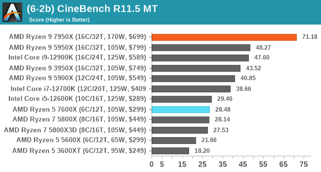
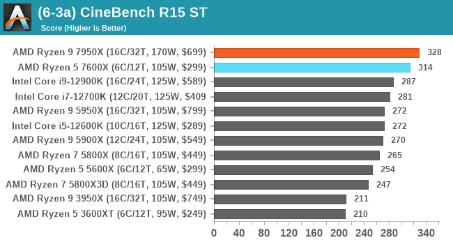
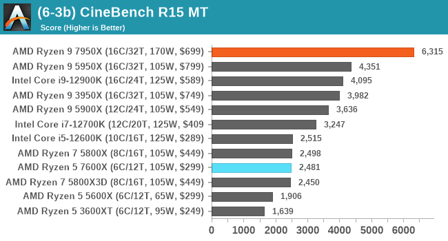
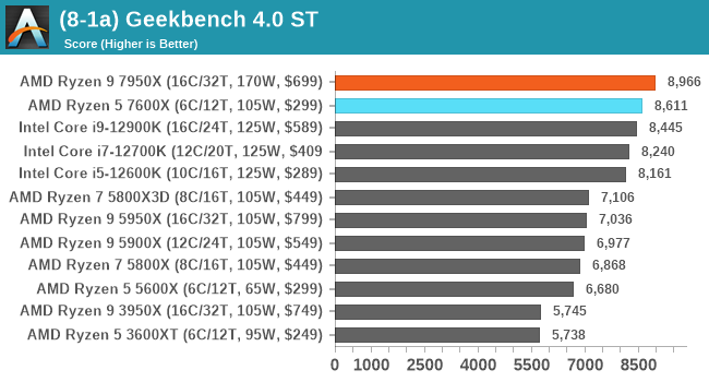
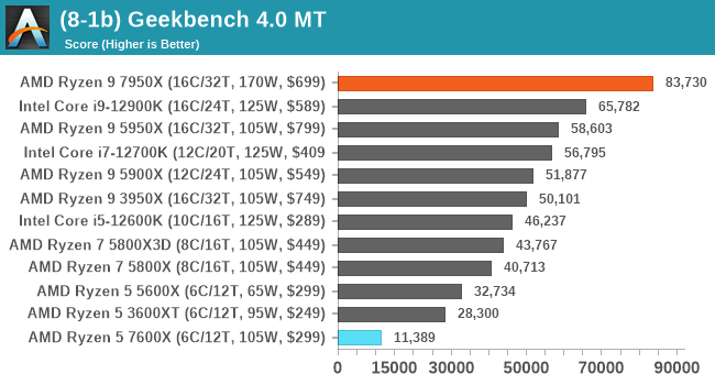
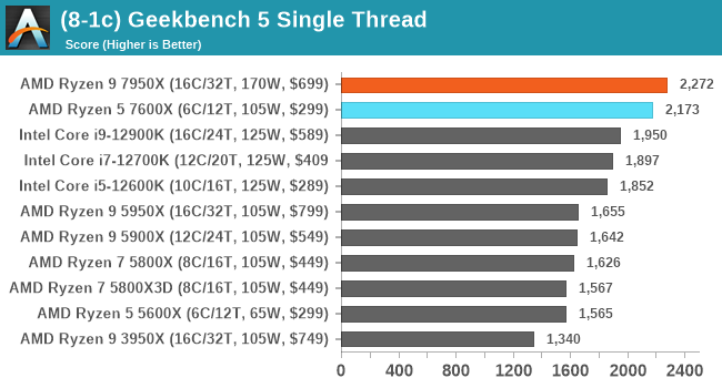
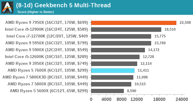
In our fabled and older school selection of benchmarks passed their 'sell by date', the Ryzen 9 7950X wins in every one of these tests, both single-threaded and multi-threaded. In the purely single-threaded tests, the Ryzen 5 7600X is the next best, although it is more in line with the Ryzen 7 5800X as we've consistently seen in our multi-threaded results all throughout this review.
All of our game testing results, including other resolutions, can be found in our benchmark database: www.anandtech.com/bench. All gaming tests here were run using integrated graphics, with a variation of 720p resolutions and at minimum settings.
We are using DDR5 memory on the Ryzen 9 7950X and Ryzen 5 7600X, as well as Intel's 12th Gen (Alder Lake) processors at the following settings:
- DDR5-5200 CL44 - Ryzen 7000
- DDR5-4800 (B) CL40 - Intel 12th Gen
All other CPUs such as Ryzen 5000 and 3000 were tested at the relevant JEDEC settings as per the processor's individual memory support with DDR4.
Civilization VI
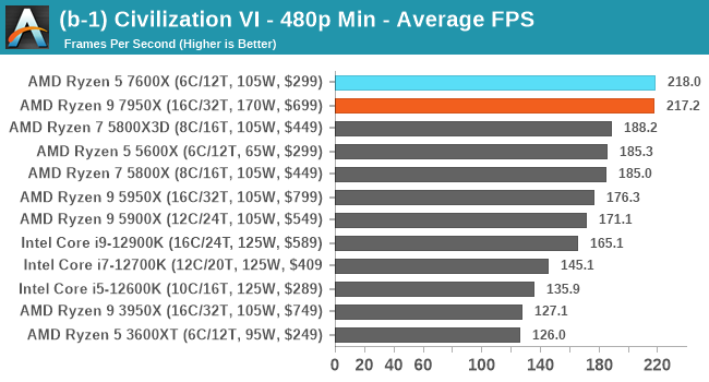
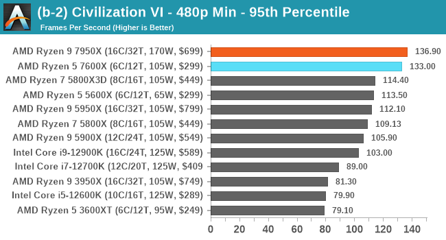
World of Tanks
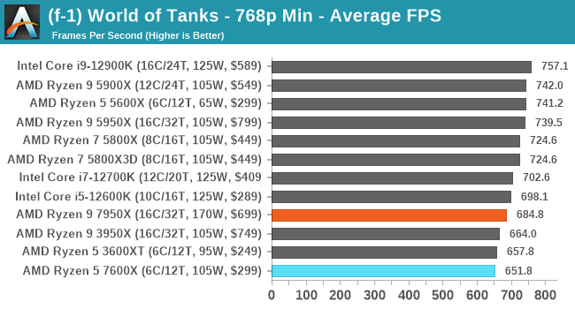
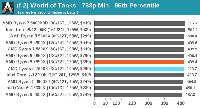
Borderlands 3
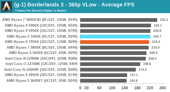
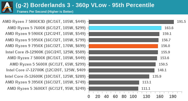
Far Cry 5
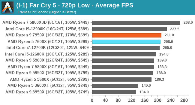
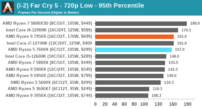
Grand Theft Auto V
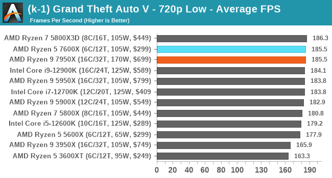
~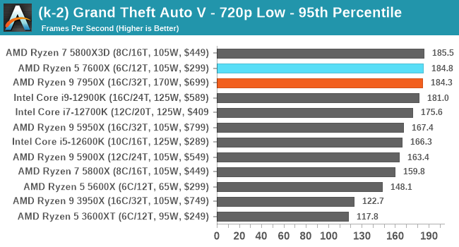
Red Dead Redemption 2
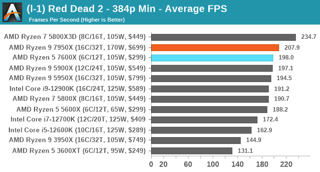
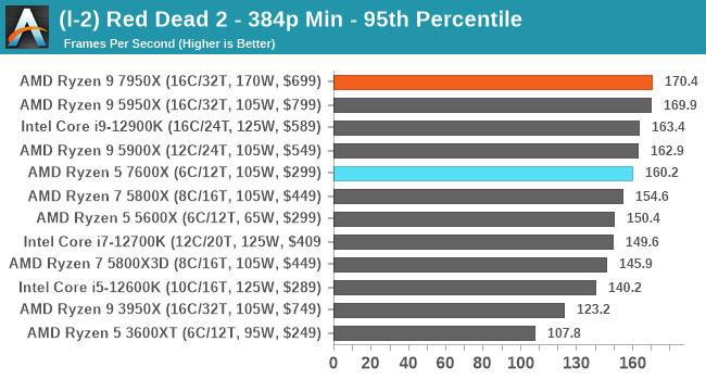
Strange Brigade (DirectX 12)
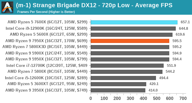
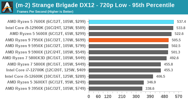
Strange Brigade (Vulcan)
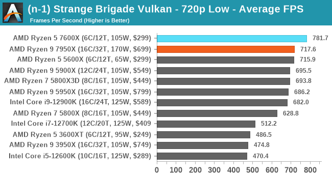
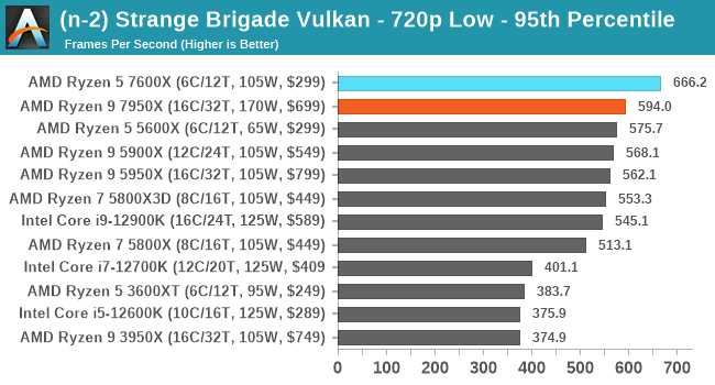
When it comes to gaming at lower resolutions such as 720p and 480p, there are more frames for the processor to, well, process, so this is where the CPU can show its limitations more so as opposed to GPU. In Civilization VI at 480p, we see the Ryzen 7950X and 7600X decimate the competition by around 15%.
What's interesting is that in some of our titles including Strange Brigade and Grand Theft Auto V, at least when using lower resolutions, the Ryzen 5 actually out performs its more expensive Ryzen 9 counterpart.
All of our game testing results, including other resolutions, can be found in our benchmark database: www.anandtech.com/bench. All gaming tests were with an RTX 2080 Ti.
We are using DDR5 memory on the Ryzen 9 7950X and Ryzen 5 7600X, as well as Intel's 12th Gen (Alder Lake) processors at the following settings:
- DDR5-5200 CL44 - Ryzen 7000
- DDR5-4800 (B) CL40 - Intel 12th Gen
All other CPUs such as Ryzen 5000 and 3000 were tested at the relevant JEDEC settings as per the processor's individual memory support with DDR4.
Civilization VI
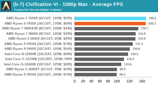
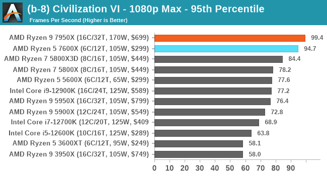
World of Tanks
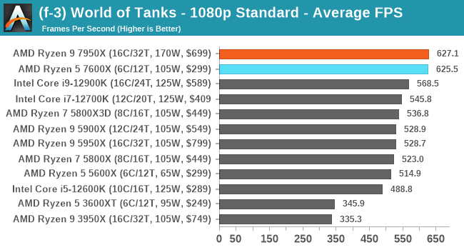
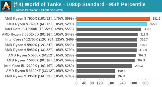
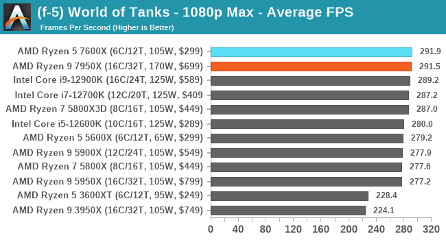
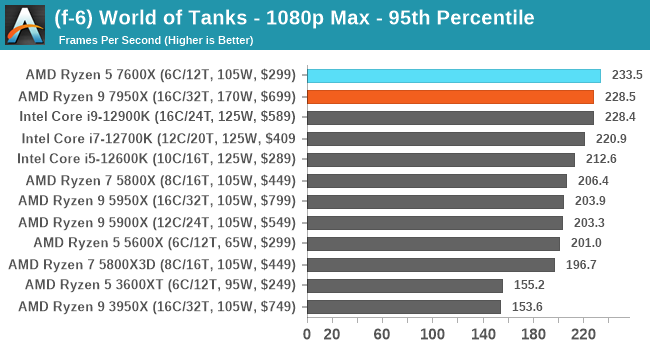
Borderlands 3

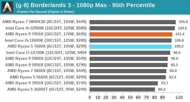
Far Cry 5
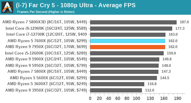
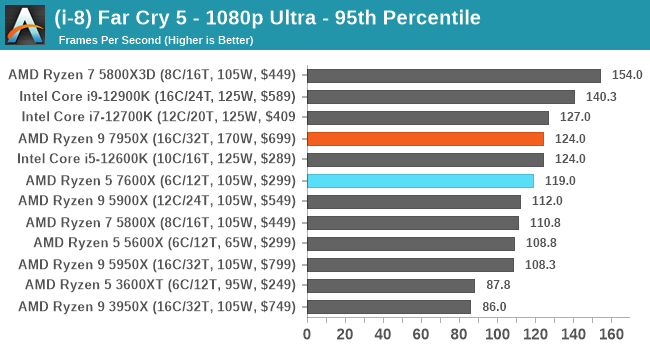
Grand Theft Auto V
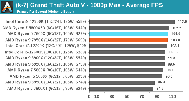
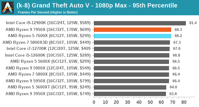
Red Dead Redemption 2
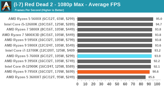
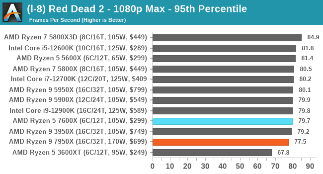
Strange Brigade (DirectX 12)
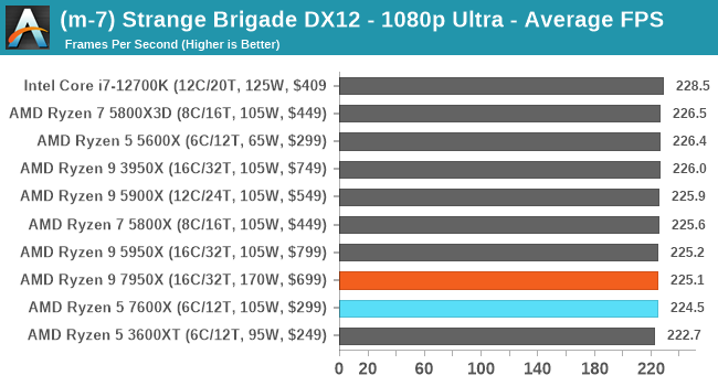
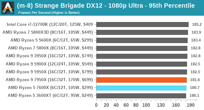
Strange Brigade (Vulcan)
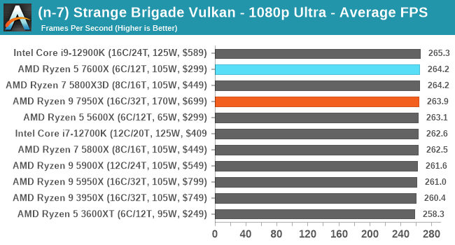
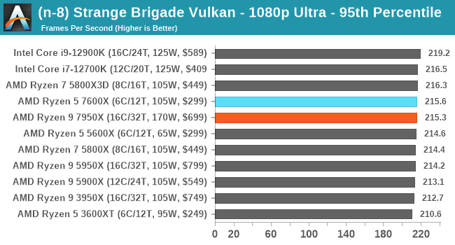
Despite modern-day graphics cards, especially the flagships, now at the level where 1440p and 4K gaming is viable, 1080p is still a very popular resolution to play games at; I have a 1440p 144Hz monitor and I play at 1080p just because that's what I'm used to.
Touching on 1080p performance with our RTX 2080 Ti, both Ryzen 7000 series chips do brilliantly in Civilization VI, as well as in World of Tanks. Over the rest of our games benchmarks (while we're testing our new ones which we will publish as soon as we're ready), performance isn't as impressive as maybe users would be expecting from a next-generation processor.
One could argue that our NVIDIA GeForce RTX 2080ti is somewhat aging and out of date, which is why we've upgraded our CPU 2023 suite with AMD Radeon RX 6950XT graphics cards. These results will be published once we've collated enough results and data points, so check back.
Summarizing 1080p performance with our current CPU 2021 suite, the Ryzen 7000 series is very competitive in gaming at 1080p, and where the CPU is required to churn more so without any bottlenecks, the Ryzen 7000's do come into their own.
All of our game testing results, including other resolutions, can be found in our benchmark database: www.anandtech.com/bench. All gaming tests were with an RTX 2080 Ti.
We are using DDR5 memory on the Ryzen 9 7950X and Ryzen 5 7600X, as well as Intel's 12th Gen (Alder Lake) processors at the following settings:
- DDR5-5200 CL44 - Ryzen 7000
- DDR5-4800 (B) CL40 - Intel 12th Gen
All other CPUs such as Ryzen 5000 and 3000 were tested at the relevant JEDEC settings as per the processor's individual memory support with appropriate kits of DDR4.
Civilization VI
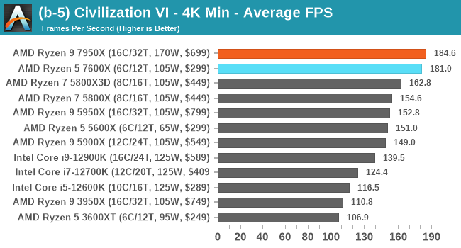
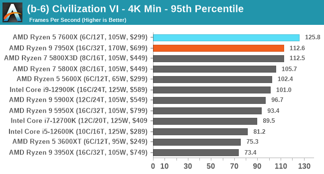
World of Tanks
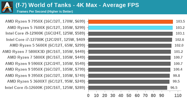
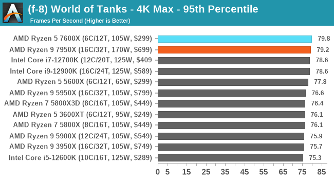
Borderlands 3
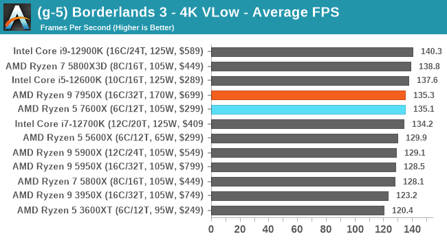
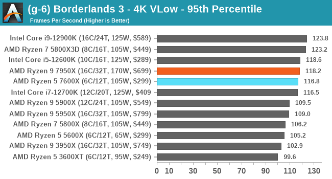
Far Cry 5
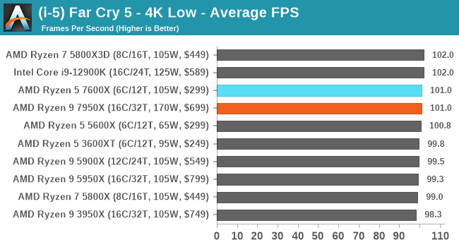
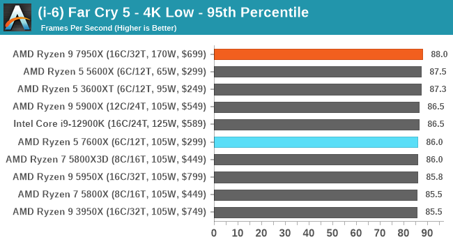
Grand Theft Auto V
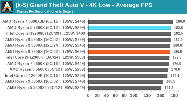
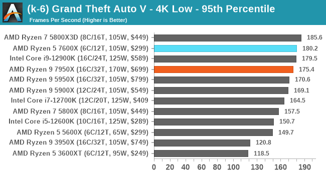
Strange Brigade (DirectX 12)
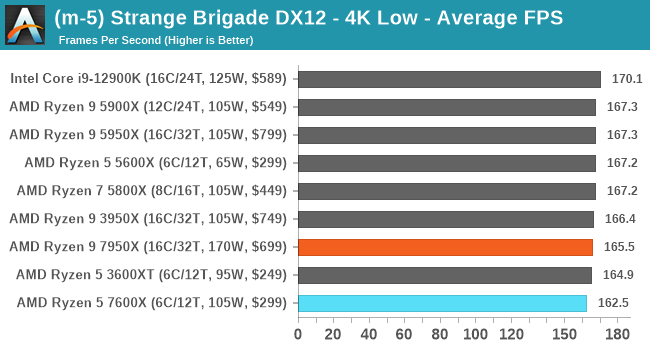
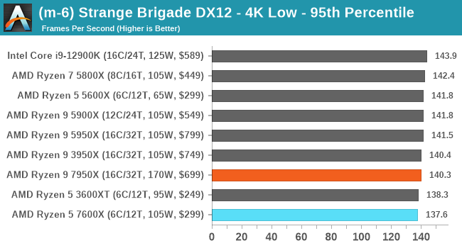
Strange Brigade (Vulcan)
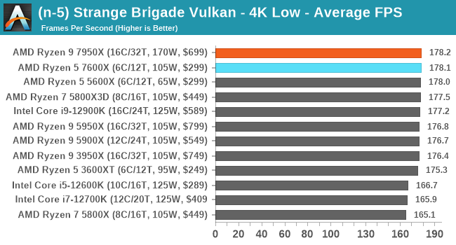
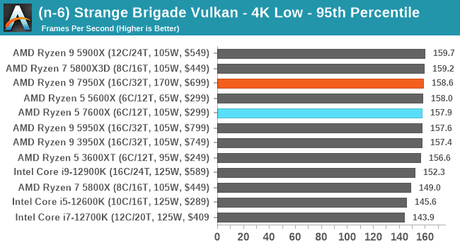
At 4K resolutions, much like our 1080p results, the Ryzen 7000 processors are very competitive, although their dominance isn't assured as it is in compute tasks such as rendering and encoding.
In World of Tanks at 4K, both Ryzen 7000 series chips perform well, while performance in the other games tested show that things look to be on an even keel; the Ryzen 7 5800X3D is still the stand-out CPU for gaming performance from AMD.
While AMD has made significant strides with Zen 4 over the previous Zen 3 and Zen 2 microarchitectures, it's time to translate these improvements into actual performance. First of all, our Ryzen 9 7950X boosted up 5.74 GHz on a single-core, which is very impressive. Although this frequency is primarily designed to increase performance throughput on single-threaded applications, the reality is that under sustained load, depending on the aggressiveness of the cooling, is more around 5.4 GHz.
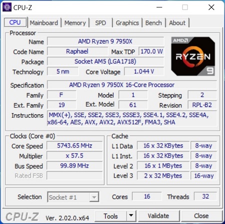
AMD's claim of an uplift of around 13% in IPC performance over Ryzen 5000 seems right on the money, and an overall improvement of 29% in single-threaded performance. Even this is still a marked improvement over AMD's Ryzen 5000 processors, which benefited from a maximum single-core boost of around 5.05 GHz, taken from our Ryzen 9 5950X and Zen 3 deep dive. In our SPEC2017 suite, we saw similar gains in single-threaded performance across various workloads.
It is in multi-threaded performance where AMD's Zen 4 based Ryzen 7950X excels. In some workloads, we saw up to an increase of 38% in multi-threaded performance in SPEC2017 nT, with others floating around the 30% mark when compared directly to the Ryzen 9 5950X (Zen 3), which is what AMD is claiming.
For the following conclusion analysis, we do test at JEDEC settings, but it's apparent that using AMD EXPO memory profiles, such as DDR5-6000, will ultimately lead to slightly higher performance in difference scenarios. If you would like us to investigate memory scaling on the Zen 4 core at some point in the future, please let us know in the comments.
A Quick Note on Temperatures: Zen 4 is Hot, But it's a Design Choice
When compared directly to the previous generation (Zen 3), AMD's Ryzen 7000 processors run quite hot; in fact in our testing, it was rare if our chips didn't hit their respective TJ Max of 95°C. The 95°C mark is where AMD has designed Ryzen 7000 to hover around, which maximizes processor performance up to this point, with frequencies scaling back with Precision Boost Overdrive.
Although AMD has said explicitly that 95°C is not the limitation, users can override this to a maximum of 115°C when manually overclocking. We feel that the higher all-core frequencies under maximum load, 95°C is a sufficient level of heat for what is on offer when it comes to overall performance. This might disgruntle users looking to use Ryzen 7000 in more tight spaces, such as small form factor systems where cooling performance is somewhat limited. Still, users can always use the incoming ECO Mode to make things more manageable (more on that down the page).
Ryzen 7000: Adding AVX-512 Support (Double Pumping With 256-bit Channels)
As we can see in our 3DPM v2.1 AVX workload test, due to AMD's implementation of its 256-bit data path, which AMD claims is to prevent thermal and frequency compromises in peak performance, the Ryzen 9 7950X and Ryzen 5 7600X both trounce the competition in AVX workloads.
Although the use case of AVX-512 is limited to specific applications such as emulation, Ryzen 7000 and Zen 4 give users looking to utilize AVX and AVX-512 a route to do so through the desktop platforms.
AMD Ryzen 7950X: Breaking 38K in CineBench R23, New World Records
In the past, AMD has broadly used CineBench as a measure of its performance; higher core and thread counts are typically favored by rendering workloads, so it's understandable why. AMD sent us a PR around its performance with the Ryzen 9 7950X breaking 48k in CineBench R23 nT at 6.45 GHz all-core using liquid nitrogen cooling. While this is impressive, and ultimately a new world record (someone will break it quickly), this isn't entirely relevant to the masses, and we're focusing on real-world everyday performance.
Looking at multi-threaded performance in CineBench R23, the AMD Ryzen 7950X achieved over 38K, which is undoubtedly impressive. Compared directly to Intel's Core i9-12900K, AMD is leading Intel here by around 42%, which is fantastic if you're looking for a desktop processor that's good at everything but excels in rendering workloads. By contrast, as the Ryzen 5 7600X is a 6C/12T chip, rendering performance isn't as impressive, but it's compatible with the Ryzen 7 5800X (8C/16T), which it competes with on a pretty consistent basis as per our testing for this review. That is impressive as it shows that six Zen 4 cores are roughly equal to eight Zen 3 cores.
Focusing our attention on gaming performance and the improvements we are seeing in our current yet soon-to-be updated CPU gaming suite aren't as fruitful as in compute-related tasks. While the AMD Ryzen 9 7950X and Ryzen 5 7600X are competitive against other CPUs such as the Core i9-12900K in the gaming sphere, there are certainly trade-offs to consider.
Looking at our result in World of Tanks using our soon-to-be-retired NVIDIA GeForce RTX 2080ti, the Ryzen 5 7600X sits at the top at 1080p Max settings regarding average frame rates. This does show that AMD's Zen 4 core is undoubtedly powerful for gaming, even at the lower end of the product stack, such as the Ryzen 5. Ultimately, the Ryzen 7000 series is trading blows with Intel's 12th Gen Core (Alder Lake) processors across many games at various settings.
Interestingly, the previous generation Ryzen 7 5800X3D with 96 MB of 3D V-Cache is also in the mix at the top end of the gaming spectrum, and despite AMD announcing that it will be releasing a Ryzen 7000-based SKU with its 3D V-Cache packaging technology, we're unfortunately going to have to wait until next year at the earliest for this. It should make for some interesting gaming results, depending on which Ryzen series it looks to capitalize on. It will be even more interesting to see how Intel, if it can, responds in the manner that the Ryzen 7 5800X3D impacted in framerates.
Looking at a more CPU-intensive gaming situation, such as at 720p in Grand Theft Auto V, the Zen 4 cores show their aggression in fighting the Core i9-12900K in terms of framerate. However, they are leapfrogged in this title by the Ryzen 7 5800X3D, which is expected as that processor is great in gaming but average at best in compute scenarios.
As we start to roll out our new CPU suite for 2023, which we're currently testing as we write this review, including some of the most current and latest game titles with more up-to-date graphics cards (Radeon 6950 XT), we will update our review with our findings to see how well the Zen 4 core compares to Zen 3, Zen 2, and Intel's 12th Gen Core. As it stands now, though, AMD's 5nm Zen 4 core hits a home run in compute performance compared to Zen 3 and Alder Lake, but it's more of a stalemate overall in terms of our game testing (so far).
Ryzen 9 7950X at 65 W (ECO Mode): Zen 4 has Superb Efficiency
Regarding power efficiency, AMD claims that their Zen 4 microarchitecture on TSMC's 5 nm node is its most efficient core to date. In light of this, AMD's ECO Mode allows users to adjust the processor limits through its Precision Boost Overdrive 2 settings, which have remained unchanged from the previous generation. The goal of ECO Mode is to restrict overall power with lower CPU VCore and lower current through the CPU socket (AM5) to reduce overall power consumption significantly. This also allows the Ryzen 7000 series to operate at lower temperatures, which is perfect for small form factor systems that can't fit in more aggressive CPU coolers while still benefiting from a large percentile of performance on offer.
AMD's Ryzen 7000 ECO Modes are as follows:
- 170W TDP Base = 105W with ECO Mode enabled
- 105W TDP Base = 65W with ECO Mode enabled
Going one step further than this, users can set their own package power tracking (PPT), thermal design current (TDC), and electrical design current (EDC) values into Ryzen Master or in the Precision Boost Overdrive (PBO) settings section of the firmware. AMD shared with us its recommended settings for 170 W, 105 W, and 65 W. The relevant settings for each of the main (170, 105, 65 W) TDP profiles AMD recommend are as follows:
- 170 W = 230,000 PPT, 160,000 TDC, and 225,000 EDC
- 105 W = 142,000 PPT, 110,000 TDC, and 170,000 EDC
- 65 W = 88,000 PPT, 75,000 TDC, and 150,000 EDC
Using CineBench R23 as our metric in determining how much performance loss there is on the Ryzen 9 7950X from its base TDP of 170 W down to 65 W, we are still seeing high-performance levels on both the single-threaded and multi-threaded tests.
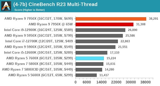
Restricting our Ryzen 9 7950X processor to just 65 W in comparison to leaving power settings untouched, the CineBench R23's multi-threaded test performance is impressive, a score of just over 31K. For comparison, the Intel Core i9-12900K only managed just under 27K at default settings, which shows that even when restricting the power proportionally down to 65 W, there's still plenty of performance available in multi-threaded situations. For reference, restricting the Ryzen 9 7950X to 65W only loses around 18-19% in CB23 MT performance; very impressive.
In the single-threaded test with CineBench R23, we only saw a drop of around 0.3%, which is negligible depending on the workload. Dropping down the overall TDP isn't as harsh on single-threaded workloads as it will be for multi-threaded workloads. ST performance remains intact mainly despite restricting overall power consumption.
The reason we used 65 W as a showcase for Zen 4's efficiency is quite simple. Restricting the power values on the Ryzen 9 7950X by around 61% (170 to 65 W) shows that the Zen 4 core is efficient and that the performance is still good. This is more relevant in small form factor systems where performance is desirable, but high heat output could impact on the longevity and performance of other components through thermal throttling.
Final Words: Zen 4 is now King, Long Live the King
Overall, when comparing AMD's new Zen 4 core to their previous Zen 3 microarchitecture, it's a big win for AMD regarding multi-threaded performance. Through the improvement of many aspects, including the switch to a higher transistor count through TSMC's 5 nm manufacturing process, higher core frequencies including both single and all-core, and the switch to DDR5 from DDR4, all of these make for a double-digit improvement to IPC performance.
| AMD Ryzen 7000 Series Processors | |||||||
| AnandTech | Cores Threads |
Base Freq |
Turbo Freq |
L2 Cache |
L3 Cache |
TDP | MSRP |
| Ryzen 9 7950X | 16C / 32T | 4.5GHz | 5.7GHz | 16 MB | 64 MB | 170 W | $699 |
| Ryzen 9 7900X | 12C / 24T | 4.7GHz | 5.6GHz | 12 MB | 64 MB | 170 W | $549 |
| Ryzen 7 7700X | 8C / 16T | 4.5GHz | 5.4GHz | 8 MB | 32 MB | 105 W | $399 |
| Ryzen 5 7600X | 6C / 12T | 4.7GHz | 5.3GHz | 6 MB | 32 MB | 105 W | $299 |
When it comes to single-threaded and multi-threaded performance, AMD takes comprehensive wins in both elements when it comes to computational workloads across the board. Although Intel's Core i9-12900K is undoubtedly a viable kit for everything, the Ryzen 9 7950X is currently the world's most powerful x86 desktop processor and delivers the performance to back it up. With an MSRP of $699, it's a cheaper insertion point than the Ryzen 9 5950X ($799) by $100, so pricing-wise, it's certainly an improvement for AMD's top-tier processor.
Touching on the Ryzen 5 7600X, this is targeted as more of an affordable processor, with similar performance levels compared to the previous generations of Ryzen 7 5800X. This in itself is an improvement, as it's essentially a 6C/12T Zen 4 processor trading blows with a Zen 3 8C/16T processor. The pricing is even more critical, as the Ryzen 5 7600X has an MSRP of just $299, making it exceptional value for money, especially from the gaming perspective. In contrast, the Ryzen 7 5800X that the 7600X trades blows with had a cost of $449 at launch back in 2020, so AMD is raising the game again in the current economic climate.
AMD has again taken the crown in overall CPU performance, so it's now Intel's turn to see how they respond. While it is expected that Intel will be retaliating in some shape or form, either that be through price cuts to its existing Alder Lake processors or the launch of its upcoming 13th Gen Core series (codenamed Raptor Lake), it has a lot of ground to make up in IPC and compute performance. At the time of writing, the AMD Zen 4 core is powerful and shows good performance efficiency at lower power levels.
https://ift.tt/tnvelTo
Technology


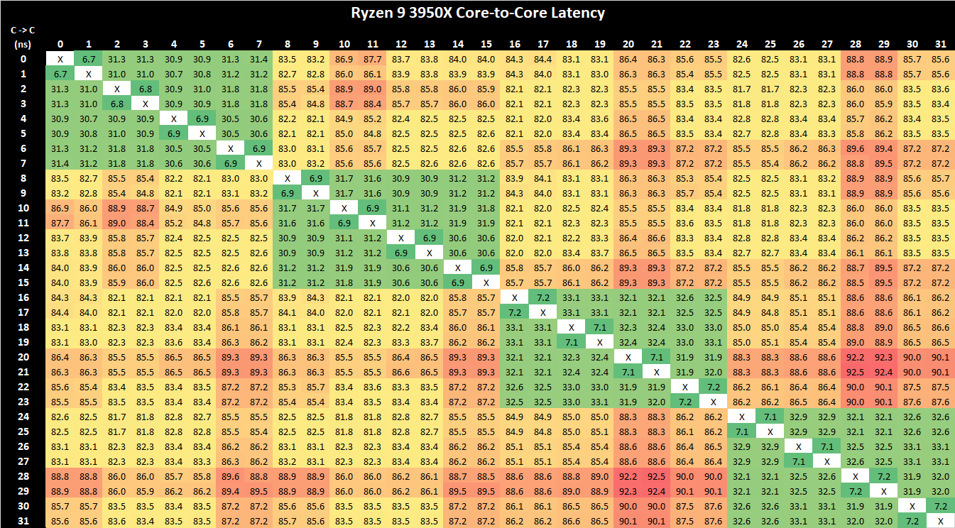
No comments:
Post a Comment